
Semiconductor inspecting apparatus

Active Publication Date: 2008-10-23
HITACHI HIGH-TECH CORP
View PDF1 Cites 7 Cited by
  • Summary
  • Abstract
  • Description
  • Claims
  • Application Information

AI Technical Summary

Benefits of technology

[0007]The present invention solves, in an apparatus including many types of data transmission systems different in required transmission capacity, a problem of a data transmission apparatus itself such as reduction in application scope due to the parallel bus width and the number of serial lanes that are fixed as described above, when the data transmission apparatus is installed in each transmission system, and a problem as the apparatus such as an increase in development costs and reduction in the reliability of transmission systems due to individual development of the data transmission apparatus, and provides a semiconductor inspecting apparatus that makes the data transmission systems within the apparatus common and is reduced in apparatus costs by realizing a data transmission apparatus and a data transmission method that have high freedom and are excellent in incorporation capability.

Problems solved by technology

A problem in this case is that the bit width of a parallel bus is fixed every 16 bits.
When it deviates to ‘1’ or ‘0’, a jitter component increases, and an increase in bit errors is caused.
For example, the parallel bus width interface cannot be freely increased or decreased in size to meet constraints of hardware.
As a result, when data transmission systems existing in a semiconductor inspecting apparatus are constituted by the number of serial lanes that achieves required transmission capacity, implementation by parallel bus width suitable for each of the data transmission systems becomes difficult, and application of a wide serial data transmission apparatus within the apparatus becomes difficult.
In this case, however, there are a problem of an increase in new development costs, and a problem that reliability is not increased because data transmission apparatuses individually developed have different circuit constructions.

Method used


Image

  • Semiconductor inspecting apparatus
  • Semiconductor inspecting apparatus
  • Semiconductor inspecting apparatus

Examples


first embodiment

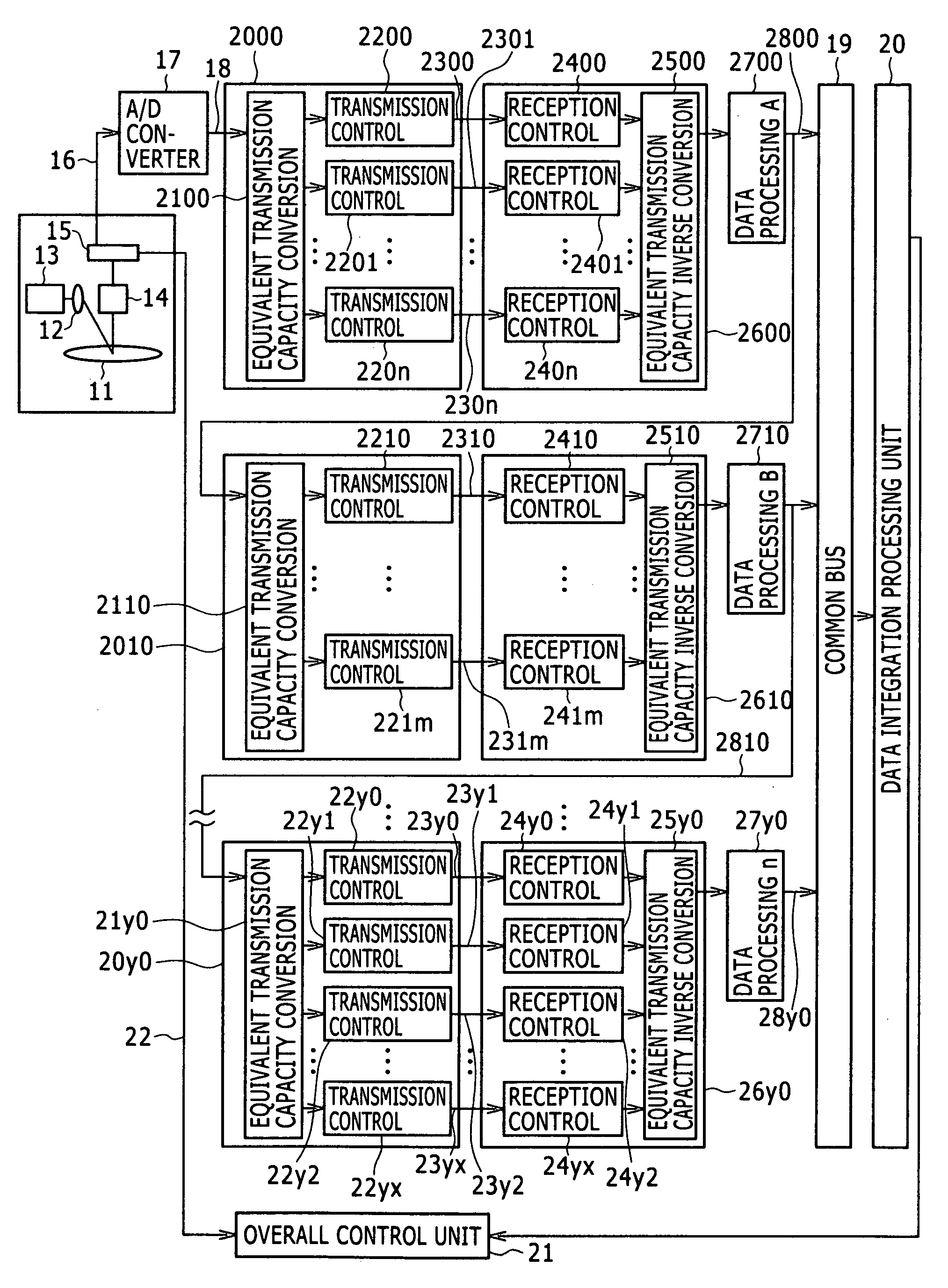
[0032]An embodiment of a semiconductor manufacturing apparatus of the present invention will be described using a semiconductor inspecting apparatus as an example with reference to the accompanying drawings.

[0033]Semiconductor inspecting apparatuses include optical ones, SEM-type appearance inspecting apparatus, SEM length measuring apparatus, and the like. A data transmission apparatus in an inspecting is required to transmit a huge amount of image data obtained from image data acquiring means.

[0034]FIG. 1 is a schematic diagram showing an embodiment of an optical appearance inspecting apparatus in an embodiment of a semiconductor manufacturing apparatus of the present invention.

[0035]Light (e.g., UV light, DUV light) emitted from a light source 13 is condensed in a slit shape by a condensing lens 12, and is irradiated onto a wafer 11 that moves to a specific direction through an objective lens.

[0036]Light reflected from a circuit pattern formed on the wafer is condensed by an obje...

second embodiment

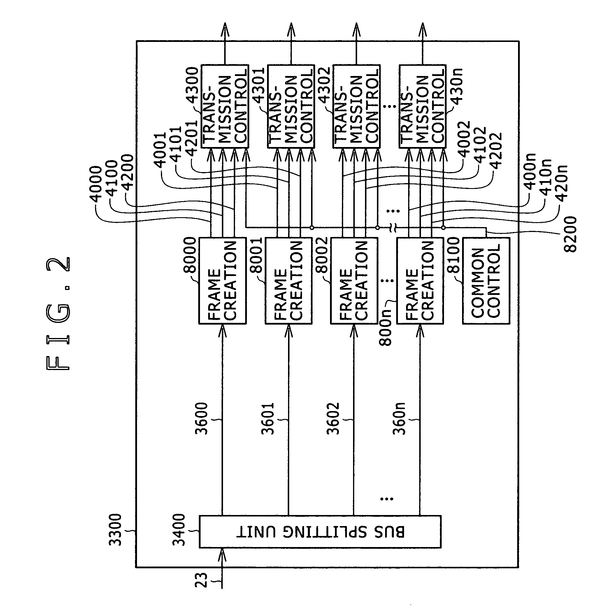
[0079]The following describes the operation of the preceding stage bus switching unit 3500 and the following bus switching unit 3900 that are shown in FIG. 4, and the operation of the preceding stage bus switching unit 4800 and the following bus switching unit 5000 that are shown in FIG. 5. The preceding stage bus switching unit and the following bus switching unit are described using an example of performing ring-shaped bus switching processing.

[0080]FIG. 10 conceptually describes the operation of ring-shaped width conversion. On the left side, 32-bit wide data is inputted to a parallel bus. In first data input 5700, the data is split to two 16-bit data by bus splitting. Likewise, as in second data input 5701 and third data input 5702, for each input cycle, the data slides on the ring by the width of the parallel bus. It is assumed that a serial transmission control unit has four lanes and 64-bit width. When the second data input 5701 is completed at the parallel bus input side, 64...

third embodiment

[0083]The shapes of serial transmission lanes generated by the equivalent transmission capacity conversion are shown in FIG. 13 on the assumption that three lanes are used with 64-bit width input and a serial transmission control unit bus width of 16 bits, and transmission is performed with a bus width of 46 bits. When seven-cycle data 6300 consisting of 64 bits is inputted from a parallel side, three transmission frames 6500, 6501, and 6502 are generated by equivalent transmission capacity conversion 6400. In the drawing, “S” designates the start of a frame, and “E” designates the end of a frame.

[0084]“E” indicates padding data added by the following stage bus switching unit, that is, invalid data. This is described below.

[0085]The following stage bus switching unit pads gaps of transmission data occurring during bus width conversion. In FIG. 13, when input is 64 bits and output is 46 bits, assume that 64-bit wide data is inputted in seven cycles. In this case, although the data is...


PUM


Abstract

A semiconductor inspecting apparatus includes: a buffer memory whose width is matched to the greater of parallel bus width and the width of the number of serial lanes; a preceding stage bus switching unit that fills the buffer memory with input data without making a free space; equivalent transmission capacity conversion including a following stage bus switching unit that fills read data to the width of an arbitrary number of serial lanes without making a free space; a preceding stage bus switching unit that fills a buffer memory with input data without making a free space; and equivalent transmission capacity inverse conversion including a following stage bus switching unit that fills a parallel bus of arbitrary width with data read from a buffer memory without making a free space.

Description

BACKGROUND OF THE INVENTION[0001]The present invention relates to a semiconductor inspecting apparatus, and more particularly to a data transmission apparatus and a data transmission method in the semiconductor inspecting apparatus.[0002]Because of the micronization of a today's semiconductor integrated circuit and the high density of substrate wirings, a circuit pattern formed on a semiconductor wafer is rapidly micronized. Accompanying with this, semiconductor inspecting apparatuses typified by a wafer appearance inspecting apparatus and a scanning electron microscope are demanded to have higher image processing power year by year. Accompanying with this, transmission capacity of image data increases, and higher data transfer speeds are desired. For example, as described in JP-A-2002-223203, in an apparatus typified by a wafer appearance inspecting apparatus and a scanning electron microscope, a huge amount of image data is serially transmitted from a transmitter to a receiver.[00...

Claims


Application Information

Patent Timeline
IPC IPC(8): G01R31/303
CPCG01N21/95684G06F13/4045
Inventor SAKURAI, YUICHITOBA, TADANOBUKIKUCHI, SHUJI
Owner HITACHI HIGH-TECH CORP
Features
  • Generate Ideas
  • Intellectual Property
  • Life Sciences
  • Materials
  • Tech Scout
  • Unparalleled Data Quality
  • Higher Quality Content
  • 60% Fewer Hallucinations
Learn More