Substrate processing apparatus and method for manufacturing semiconductor device

a technology of substrate processing and semiconductor devices, applied in vacuum evaporation coatings, chemical vapor deposition coatings, coatings, etc., can solve the problems of short service life, poor performance of semiconductor devices manufactured on substrates on which foreign matter is adsorption, and participation in contamination, etc., to suppress foreign matter agitation and foreign matter

Active Publication Date: 2008-10-30
KOKUSA ELECTRIC CO LTD
View PDF19 Cites 521 Cited by
  • Summary
  • Abstract
  • Description
  • Claims
  • Application Information

AI Technical Summary

Benefits of technology

[0016]The present invention makes it possible to provide a substrate processing apparatus and a method for manufacturing a semiconductor device where

Problems solved by technology

Byproducts that accumulate in the processing chamber in the course of substrate processing may also participate in contamination.
A film can easily form on the inside wall of the processing chamber or on members inside the processing chamber particularly during the substrate processing step of forming a thin film on the substrate, and contaminants can be f

Method used


Image

  • Substrate processing apparatus and method for manufacturing semiconductor device
  • Substrate processing apparatus and method for manufacturing semiconductor device
  • Substrate processing apparatus and method for manufacturing semiconductor device

Examples


first embodiment

1. First Embodiment of the Present Invention

[0034]The structure of a processing oven 202 of a substrate processing apparatus as the first embodiment of the present invention, a substrate processing step performed through the use of the processing oven 202 as a step in a semiconductor device manufacturing process, and an example of the cyclic processing performed in the substrate processing step will be described in sequence hereinafter.

(1) STRUCTURE OF THE PROCESSING OVEN

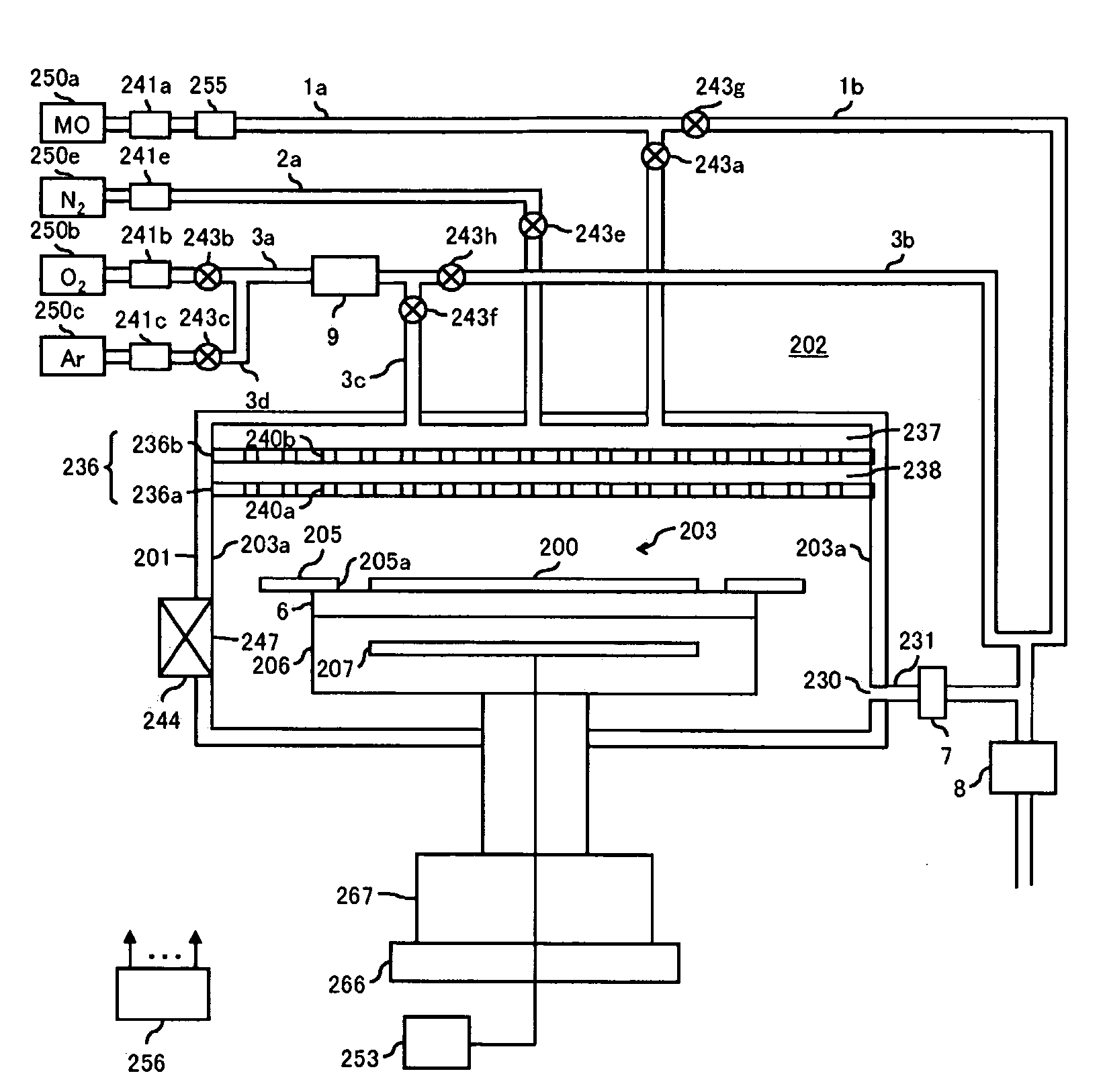
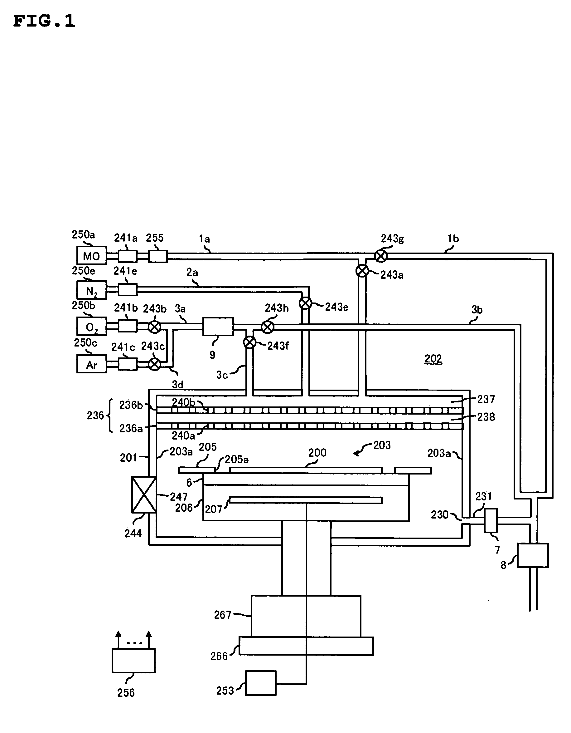
[0035]The structure of the processing oven 202 of the substrate processing apparatus as the first embodiment of the present invention will first be described using FIG. 1. FIG. 1 is a schematic view showing an example of the processing oven of a single-wafer MOCVD device, which is the substrate processing apparatus according to the first embodiment of the present invention.

Processing Vessel

[0036]The processing oven 202 according to the present embodiment is provided with a processing vessel 201. The processing vesse...

example

[0091]In contrast, as a result of concentrated investigation, the inventors discovered that even if a substrate processing apparatus having the structure shown in FIG. 1 is used, it is still possible to suppress pressure fluctuations from occurring within the processing chamber 203 if the supply of gases is controlled as in the example described below.

[0092]FIG. 4B is a detailed sequence chart showing an example of the cyclic processing according to the first embodiment, which is able to suppress pressure fluctuations from occurring within the processing chamber 203.

[0093]As shown in FIG. 4B, the cyclic processing of the present example has the following steps as one cycle: (1) feeding of a source obtained by activating an MO source material, and feeding of an inert gas (N2 gas) (source gas feeding step); (2) feeding of an inert gas (purge step); (3) feeding of an activated gas (O2 / Ar mixed gas) obtained by activating an oxidizing agent (O2), and feeding of an inert gas (activated g...

second embodiment

2. Second Embodiment of the Present Invention

[0102]The structure of the processing oven 202 of the substrate processing apparatus as the second embodiment of the present invention, and an example of the cyclic processing in the substrate processing step performed by the processing oven 202 will next be described in sequence.

(1) Structure of the Processing Oven

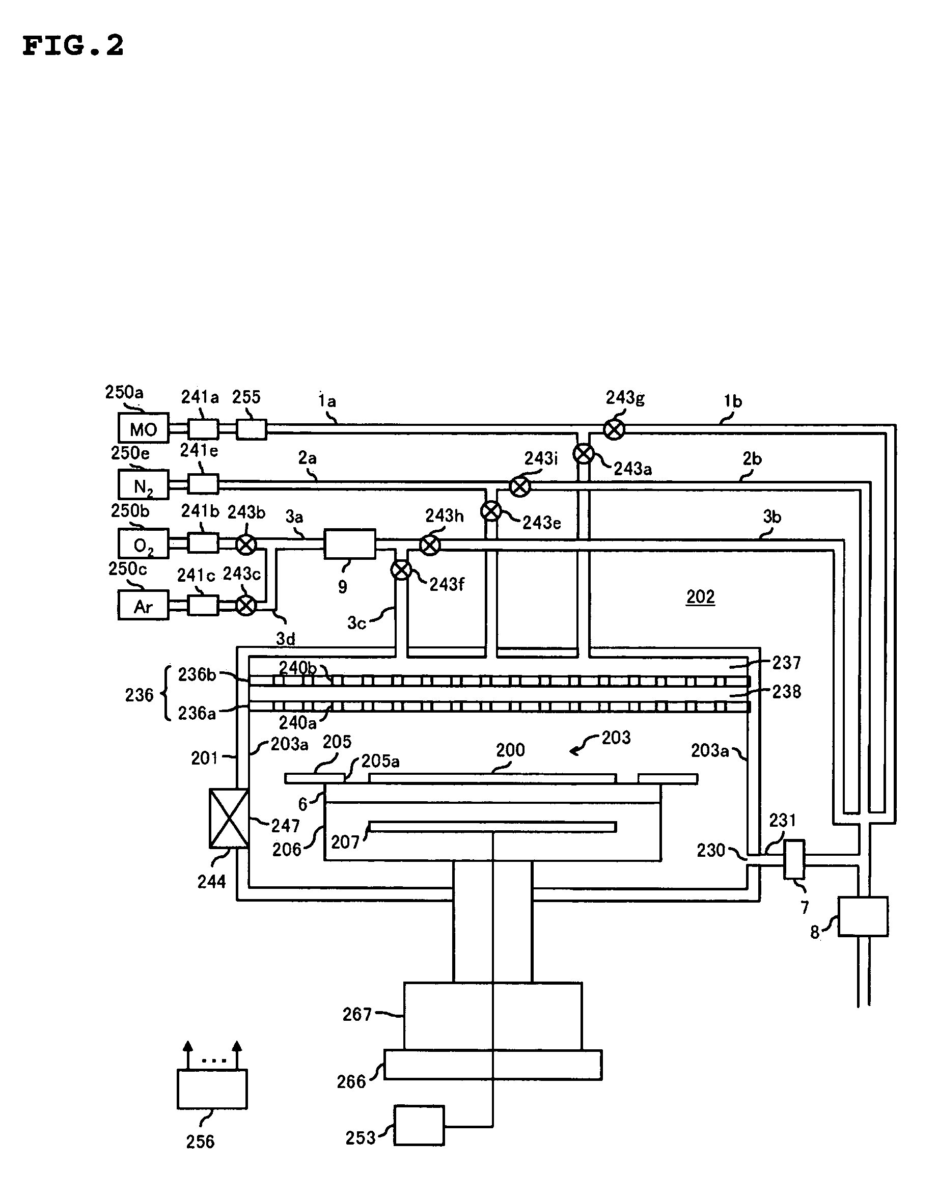
[0103]The structure of the processing oven of the substrate processing apparatus as the second embodiment of the present invention will first be described using FIG. 2. FIG. 2 is a schematic view showing an example of the processing oven of a single-wafer MOCVD device, which is the substrate processing apparatus according to the second embodiment of the present invention.

[0104]The processing oven 202 of the second embodiment differs from the processing oven 202 of the first embodiment in that an inert gas vent duct 2b is provided as an inert gas vent line not only to the source gas supply duct 1a and the activated gas feeding d...


PUM

PropertyMeasurementUnit
Flow rateaaaaaaaaaa

Abstract

A substrate processing apparatus and a method for manufacturing a semiconductor device whereby foreign matter can be prevented from being adsorbed on the substrate, by suppressing agitation of foreign matter present in the processing chamber. The substrate processing apparatus comprises a processing chamber for processing a substrate; a processing gas feeding line for feeding a processing gas into the processing chamber; an inert gas feeding line for feeding an inert gas into the processing chamber; an inert gas vent line provided in the inert gas feeding line, for exhausting the inert gas fed into the inert gas feeding line without feeding the inert gas into the processing chamber; a first valve provided in the inert gas feeding line, on a downstream side of a part where the inert gas vent line is provided in the inert gas feeding line; a second valve provided in the inert gas vent line; and an exhaust line that exhausts an inside of the processing chamber.

Description

BACKGROUND OF THE INVENTION[0001]1. Field of the Invention[0002]The present invention relates to a substrate processing apparatus and to a method for manufacturing a semiconductor device.[0003]2. Description of the Related Art[0004]A case such as executing a substrate processing step of forming a thin film on a processed substrate such as a silicon wafer, is given as an example, as a step of the manufacturing step of the semiconductor device such as an LSI. Such physical vapor deposition (PVD) methods as sputtering and the like, or a chemical vapor deposition (CVD) method using a chemical reaction, for example, are sometimes performed in the substrate processing step of forming the thin film on the substrate. Since the CVD method generally possess advantages not had by the PVD method, such as step coverage characteristics, the CVD method is widely employed as a film formation method.[0005]The substrate processing step described above is executed by a substrate processing apparatus p...

Claims


Application Information

Patent Timeline
IPC IPC(8): C23C16/52C23C14/34H01L21/00
CPCY10T29/41C23C16/4408
Inventor SANO, ATSUSHIITATANI, HIDEHARUTANABE, MITSURO
Owner KOKUSA ELECTRIC CO LTD
Why Eureka
Try Eureka