
Liquid crystal display device and manufacturing method

Active Publication Date: 2008-10-30
SEMICON ENERGY LAB CO LTD
View PDF3 Cites 29 Cited by
  • Summary
  • Abstract
  • Description
  • Claims
  • Application Information

AI Technical Summary

Benefits of technology

[0009]It is an object of the present invention to provide a liquid crystal display device in which deterioration of liquid crystal caused in a manufacturing process is prevented and which has good adhesion between substrates, high reliability and high image quality. It is another object of the present invention to provide a technique by which such a liquid crystal display device with high reliability and high image quality is manufactured with high productivity.
[0010]According to a feature of the present invention, in a liquid crystal display device, a plurality of projections are provided in a sealant adhesive region over a substrate and a pair of substrates are attached to each other so that the plurality of projections is implanted in the sealant. Since an area in which the sealant is in contact with the substrates is increased by the plurality of projections which is implanted in the sealant, a pair of the substrates are attached more firmly to each other and adhesion is improved.

Problems solved by technology

However, when a liquid crystal dropping method is used, since an uncured sealant and liquid crystal is in contact with each other, there has been a problem in that the liquid crystal is contaminated by the sealant and a sealant with little contamination of liquid crystal has been developed (for example, see Patent Document 2: Japanese Published Patent Application No. 2005-115255).

Method used


Image

  • Liquid crystal display device and manufacturing method
  • Liquid crystal display device and manufacturing method
  • Liquid crystal display device and manufacturing method

Examples


embodiment mode 1

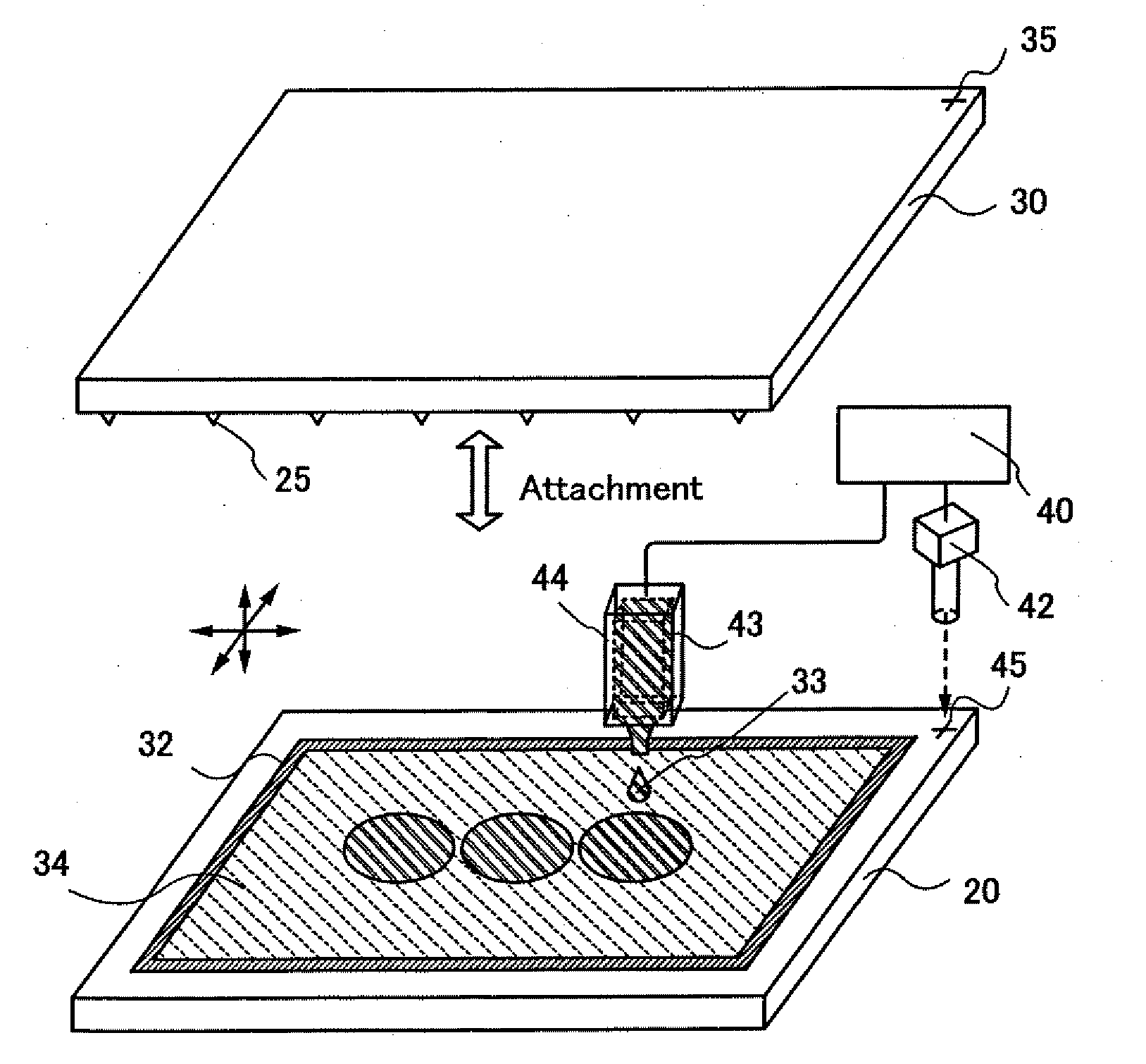
[0050]In this embodiment mode, an example of a liquid crystal display device in which deterioration of liquid crystal caused in a manufacturing process is prevented and which has higher reliability, higher image quality, and good adhesion between substrates, and the manufacturing method thereof will be described.

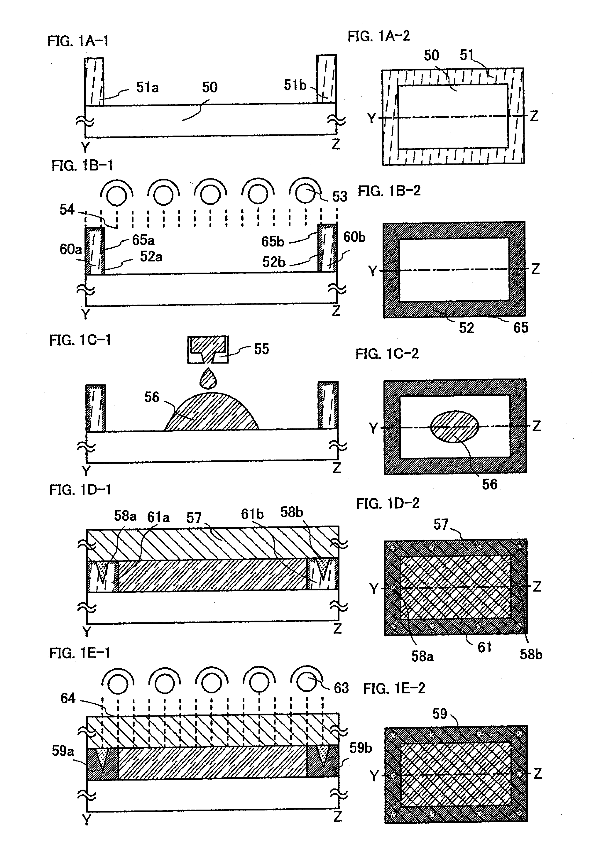
[0051]FIGS. 1A-1 to 1E-2 illustrate a method for manufacturing a liquid crystal display device in this embodiment mode using the present invention. FIGS. 1A-2 to 1E-2 are top views of a liquid crystal display device in this embodiment mode. FIGS. 1A-1 to 1E-1 are cross sectional views taken along lines Y-Z of FIGS. 1A-2 to 1E-2, respectively.

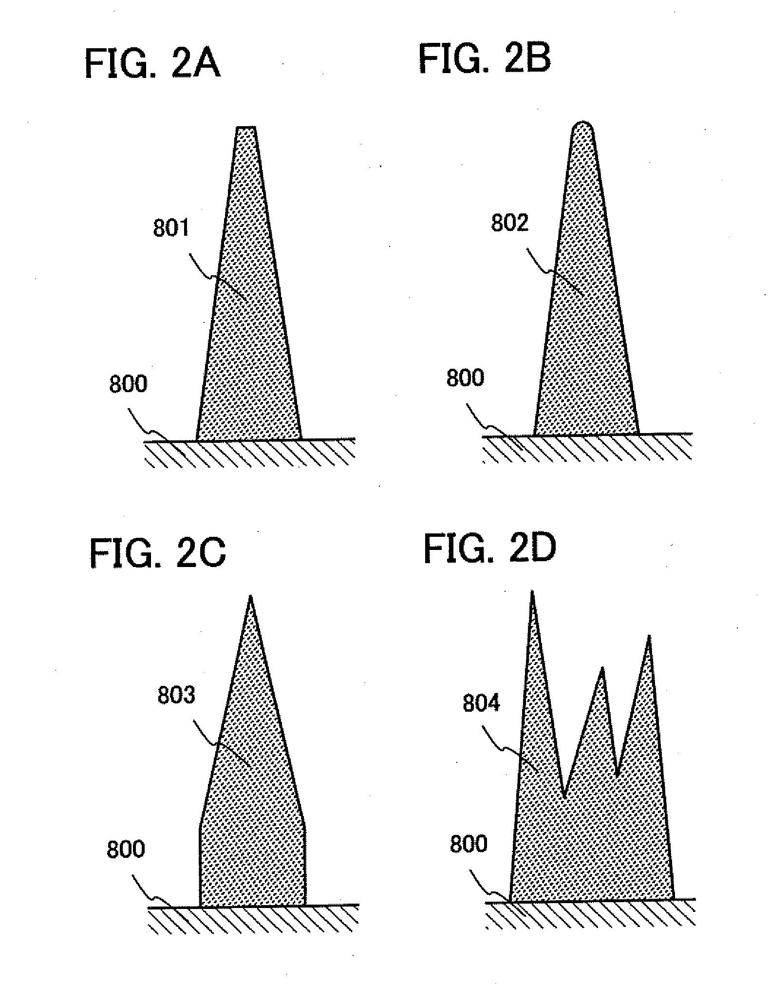
[0052]In FIGS. 1A-1 and 1A-2, an uncured sealant 51 (51a and 51b) is formed to have a frame-shaped seal pattern over a first substrate 50. In this embodiment mode, an example is described in which an ultraviolet curing resin is used as the sealant 51; therefore, the sealant 51 (51a and 51b) is irradiated with ultraviolet rays (also refer...

embodiment mode 2

[0081]In this embodiment mode, an example of a liquid crystal display device in which deterioration of liquid crystal caused in a manufacturing process is prevented and which has higher reliability, higher image quality, and good adhesion between substrates, and the manufacturing method thereof will be described. Specifically, a case in which a structure of the liquid crystal display device is a passive matrix type will be described.

[0082]FIGS. 5A and 5B illustrate a passive matrix liquid crystal display device in this embodiment mode using the present invention. FIG. 5A is a top view of the liquid crystal display device, and FIG. 5B is a cross sectional view taken along a line A-B in FIG. 5A. In FIG. 5A, an insulating layer 1704 serving as an alignment film, a colored layer 1706, a counter substrate 1710, a polarizing plate 1714, and the like are omitted and are not illustrated; however they are provided as illustrated in FIG. 5B.

[0083]In FIGS. 5A and 5B, a substrate 1700 provided ...

embodiment mode 3

[0107]In this embodiment mode, an example of a liquid crystal display device in which deterioration of liquid crystal caused in a manufacturing process is prevented and which has higher reliability, higher image quality, and good adhesion between substrates, and the manufacturing method thereof will be described. In this embodiment mode, a liquid crystal display device having a different structure from that described in Embodiment Mode 2 will be described. Specifically, a case in which a structure of the liquid crystal display device is an active matrix type will be described.

[0108]FIG. 6A is a top view of a liquid crystal display device, and FIG. 6B is a cross sectional view of a liquid crystal display device taken along a line E-F in FIG. 6A. In FIG. 6A, a liquid crystal layer, an alignment film which is provided for a counter substrate side, a counter electrode layer, a colored layer, and the like are omitted and are not illustrated; however, they are provided as illustrated in F...


PUM


Abstract

In a method for manufacturing a liquid crystal display device in which a liquid crystal layer is formed by dropping liquid crystal by a dropping method, a surface of a sealant which is formed over a first substrate is cured by a first cure treatment before dropping the liquid crystal, and then the liquid crystal is dropped. A second substrate has a plurality of projections in a sealant adhesive region. The first substrate and the second substrate are attached to each other with the liquid crystal interposed therebetween so that the plurality of projections is in contact with an uncured region in the sealant formed over the first substrate.

Description

BACKGROUND OF THE INVENTION[0001]1. Field of the Invention[0002]The present invention relates to a liquid crystal display device and a manufacturing method thereof.[0003]2. Description of the Related Art[0004]In recent years, a liquid crystal display device is used in a wide range of fields such as a liquid crystal television, a PDA, a mobile phone, and office automation equipment like a personal computer, as well as a clock and a calculator.[0005]In a liquid crystal display device, liquid crystal is sealed between two substrates. When voltage is applied, an orientation of liquid crystal molecules is changed and light transmittance thereof is changed, so that an image or the like is displayed optically.[0006]An image quality and reliability of the liquid crystal display device are largely affected by whether the two substrates are attached to each other with good adhesion with the same interval or not. A technique to reduce unevenness of a sealant caused by a wiring which is under t...

Claims


Application Information

Patent Timeline
IPC IPC(8): G02F1/1339H01J9/20
CPCG02F1/1339G02F2001/13415G02F1/1341G02F1/13415
Inventor NISHI, TAKESHIISHITANI, TETSUJI
Owner SEMICON ENERGY LAB CO LTD
Features
  • Generate Ideas
  • Intellectual Property
  • Life Sciences
  • Materials
  • Tech Scout
  • Unparalleled Data Quality
  • Higher Quality Content
  • 60% Fewer Hallucinations
Learn More