Planar Lightwave Circuit, Design Method for Wave Propagation Circuit, and Computer Program

a technology of wave propagation circuit and planar light wave, applied in the direction of optical waveguide light guide, instruments, optics, etc., can solve the problems of light field which can be realized, lightwave circuit cannot be utilized as a transmission type device, and fabrication is very difficult, so as to achieve easy fabricated effect and low loss

Active Publication Date: 2008-11-06
NIPPON TELEGRAPH & TELEPHONE CORP
View PDF11 Cites 15 Cited by
  • Summary
  • Abstract
  • Description
  • Claims
  • Application Information

AI Technical Summary

Benefits of technology

[0043]According to the invention, there is provided a planar lightwave circuit including an arrayed waveguide grating filter, which can be easily fabricated by an existing planar-lightwave-circuit fabrication process, and which is of low loss.

Problems solved by technology

Regarding the prior-art planar lightwave circuit which is designed with the propagation mode of the optical waveguide set at the fundamental mode as described in connection with FIG. 40, there has been the problem that a light field which can be realized is limited, and regarding the prior-art planar lightwave circuit whose function is realized by the segmentation of the optical waveguide, there has been the problem that the reflected light, etc. appear due to the abrupt variation of the waveguide width, so the lightwave circuit cannot be utilized as a transmission type device.
These planar lightwave circuits have had the problem that very fine optical waveguides need to be realized, so the fabrications are very difficult.
Besides, the lightwave circuit which includes the prior-art cross waveguide as described in connection with FIG. 41 has had the problem that the optical coupling loss in the optical-waveguide crossing portion is heavy.
On this occasion, the higher-order mode of the signal light is excited in the optical-waveguide branching portion 372, resulting in the problem that the optical coupling loss of the signal light enlarges.
Also, there has been the drawback that the branching ratio of the signal light deviates from a desired design value and becomes unstable due to the appearance of the higher-order mode mentioned above.
Besides, the prior-art optical branch circuit has had the drawback that, also in a case where the first-order mode mixes in the signal light, in addition to the fundamental mode, the actual branching ratio deviates from the desired design value, so the precision of the branching ratio degrades much.

Method used


Image

  • Planar Lightwave Circuit, Design Method for Wave Propagation Circuit, and Computer Program
  • Planar Lightwave Circuit, Design Method for Wave Propagation Circuit, and Computer Program
  • Planar Lightwave Circuit, Design Method for Wave Propagation Circuit, and Computer Program

Examples


first embodiment

[0106]The first embodiment of the invention will be described with reference to FIGS. 1 and 2.

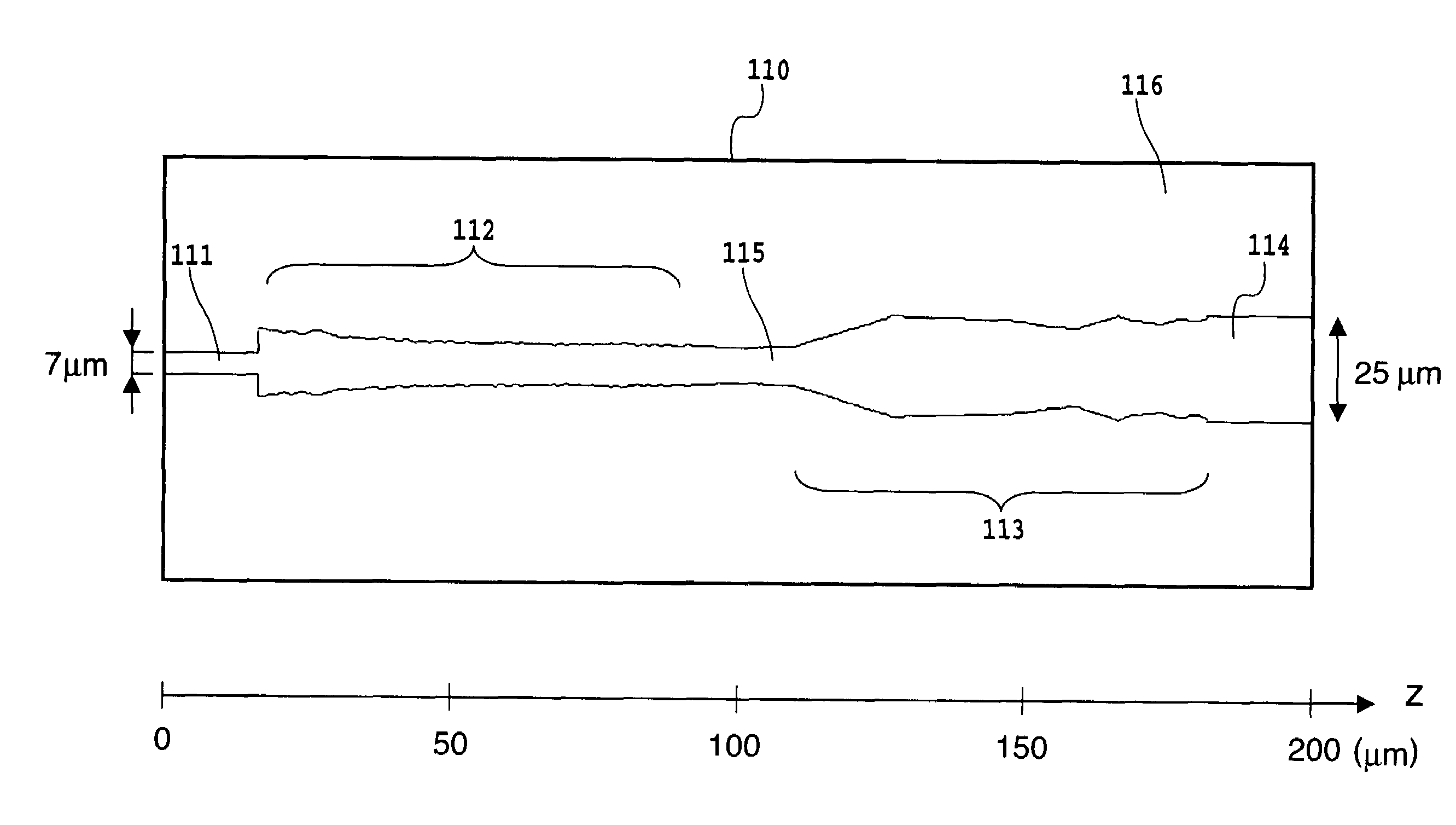
[0107]FIG. 1 is a plan view in which an optical waveguide lens (planar lightwave circuit) according to the first embodiment is seen in a direction perpendicular to a substrate. A z-axis indicates the propagation direction of signal light. Here, the optical waveguide lens is supposed in FIG. 1, and this is because the planar lightwave circuit according to the invention is excellent for realizing the lens or the like function which is difficult to be realized by only a propagation mode. However, the planar lightwave circuit according to the invention is not restricted to this embodiment, but it can be configured as a planar lightwave circuit having another function, such as spot size converter.

[0108]As shown in FIG. 1, the optical waveguide lens (planar lightwave circuit) according to the first embodiment is configured of an input optical waveguide 111 which inputs the signal light, mode coup...

second embodiment

[0120]Next, the second embodiment of the present invention will be described with reference to FIG. 3.

[0121]An optical waveguide lens (planar lightwave circuit) according to the second embodiment is a modification to the optical waveguide lens (planar lightwave circuit) according to the first embodiment.

[0122]FIG. 3 is a plan view in which the optical waveguide lens (planar lightwave circuit) according to the second embodiment is seen in a direction perpendicular to a substrate. A z-axis indicates the propagation direction of signal light. Mode coupling means 112 and mode re-coupling means 113 are configured unitarily as mode coupling / re-coupling means 131. Incidentally, the modulated core width of a waveguide can be formed by the same method as that of the optical waveguide lens (planar lightwave circuit) of the first embodiment.

[0123]As shown in FIG. 3, the mode coupling means 112 and the mode re-coupling means 113 need not have the configurations independent of each other as show...

third embodiment

[0124]Next, the third embodiment will be described with reference to FIGS. 4 through 6.

[0125]Whereas the above embodiments have indicated the examples of the planar lightwave circuits in each of which the core width of the optical waveguide is varied in the direction parallel to the substrate, a planar lightwave circuit in the third embodiment according to the invention indicates an example in which the core width of a waveguide is varied in a direction perpendicular to a substrate, that is, in a depthwise direction.

[0126]Even when the core width of the waveguide is varied in the direction perpendicular to the substrate, similar advantages can be attained. Signal light has the property that a distribution is more liable to spread in the depthwise direction. Therefore, when the core width is varied in the depthwise direction, a rather greater advantage is attained, that is, the advantage of lowering a loss attendant upon propagation is enhanced.

[0127]Shown in FIGS. 4 and 5 is the exa...


PUM


Abstract

A planar lightwave circuit is provided which can be easily fabricated by an existing planar-lightwave-circuit fabrication process, which can lower the propagation loss of signal light and which can convert inputted signal light so as to derive desired signal light. A planar lightwave circuit having a core and a clad which are formed on a substrate, has input optical waveguide(s) (111) which inputs signal light, mode coupling part (112) for coupling a fundamental mode of the inputted signal light to a higher-order mode and/or a radiation mode, or mode re-coupling part (113) for re-coupling the higher-order mode and/or the radiation mode to the fundamental mode, and output optical waveguide(s) (114) which outputs signal light. The mode coupling part or the mode re-coupling part is an optical waveguide which has core width and/or height varied continuously.

Description

TECHNICAL FIELD[0001]The present invention relates to a planar lightwave circuit for converting inputted signal light and deriving desired signal light, a design method for optimizing a wave propagation circuit, and a computer program for executing the design method.BACKGROUND ART[0002]With the still larger capacity and higher speed of an optical communication system, it has become more important to provide an optical device which carries out advanced functions at a low price. Since a lightwave circuit fabricated on a planar substrate is highly versatile in design and is excellent in mass-producibility and stability, it can provide the optical device meeting the requirement, and researches and developments have therefore been made worldwidely.[0003]Examples of prior-art planar lightwave circuits are shown in FIGS. 40 through 42. The planar circuit shown in FIG. 40 is configured of an input optical waveguide 171, and an output optical waveguide 172 which is optically coupled to the i...

Claims


Application Information

Patent Timeline
Patent Type & Authority Applications(United States)
IPC IPC(8): G02B6/12
CPCG02B6/12011G02B6/1228G02B6/2804G02B6/14
Inventor SAIDA, TAKASHISAKAMAKI, YOHEIHASHIMOTO, TOSHIKAZUKITOH, TSUTOMUTAKAHASHI, HIROSHIYANAGISAWA, MASAHIROSUZUKI, SENICHIHIDA, YASUHIROISHII, MOTOHAYATAMURA, MUNEHISA
Owner NIPPON TELEGRAPH & TELEPHONE CORP
Why Eureka
Try Eureka