Method of the Application of a Zinc Sulfide Buffer Layer on a Semiconductor Substrate

US20080274577A1Inactive Publication Date: 2008-11-06HELMHOLTZ ZENT BERLIN FUER MATERIALIEN & ENERGIE GMBH

Image

  • Method of the Application of a Zinc Sulfide Buffer Layer on a Semiconductor Substrate
  • Method of the Application of a Zinc Sulfide Buffer Layer on a Semiconductor Substrate
  • Method of the Application of a Zinc Sulfide Buffer Layer on a Semiconductor Substrate

Examples


Embodiment Construction

[0030]The following layer structure was exemplarily chosen for a chalcopyrite thin-film solar cell (no module).

Substrate:GlassRear Contact Layer:MolybdenumAbsorber:CuInS2Buffer Layer:ZnSWindow Layer:i-ZnO / ZnO:GaLight-side Contact:NiAl

[0031]For applying ZnS to chalcopyrite absorbers the samples 1 are stored in a solution of ammonia and water prior to the chemical bath deposition.

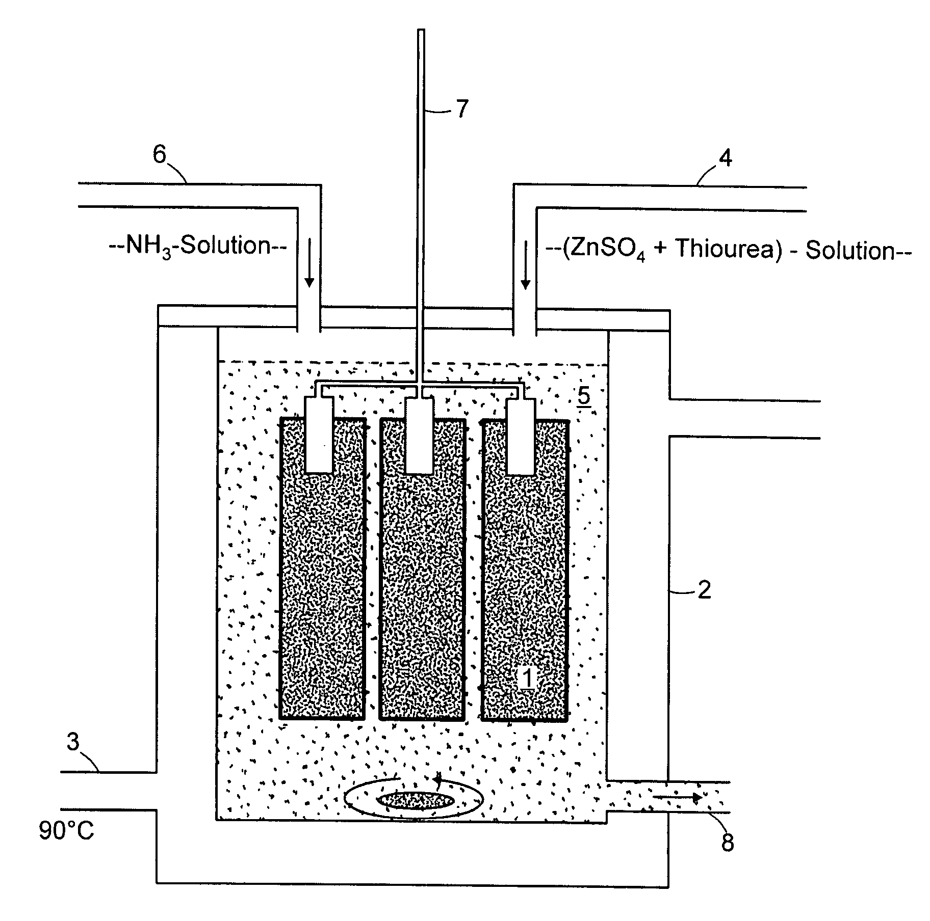
[0032]FIG. 1 depicts the structure of the test. A sample vessel 2 provided with a heater 3 is used.

[0033]The chemical bath depicted in FIG. 1 is prepared as follows:[0034]1) A hot solution (70-m90° C.) with 0.05 to 0.5 mol / l zinc sulfate and 0.2 to 1.5 mol / l thiourea is prepared with twice-distilled water (indicated by feed line 4).[0035]2) This solution is stirred for some time.[0036]3) NH3 solution (25%) is then added (indicated by feed line 6). A white precipitate can be observed at once; it is dissolved again by continuous stirring. A complete clear solution with a pH value of 10 to 11 results.[0037]4) Th...


PUM

PropertyMeasurementUnit
Temperatureaaaaaaaaaa

Abstract

A chemical bath deposition method of depositing on a semiconductor substrate a layer of zinc sulfide by dipping the semiconductor substrate into an aqueous solution of zinc sulfate and thiourea and ammonia.

Description

[0001]Chemical bath deposition (CBD) has proved top be the most favourable method for application of a buffer layer to semiconductor substrates, for example, chalcopyrite thin-film solar cells, whereby previously cadmium sulphide (CdS) was deposited and as cadmium is a highly toxic heavy metal, alternatives have been required. According to the invention, the semiconductor substrate is dipped in a solution for approximately 10 minutes, produced by the dissolution of zinc sulphate (0.05-0.5 mol / l) and thiourea (0.2 to 1.5 mol / ml) in distilled water at a temperature being held essentially constant throughout said period. For the first time, the ZnS layer permits comparable or higher efficiencies than conventionally only achieved with toxic cadmium compounds. The method is hence much more environmentally-friendly with the same result.BACKGROUND OF THE INVENTION[0002]1. Field of the Invention[0003]The invention, in general, relates to a novel method of applying a zinc sulfide buffer laye...

Claims


Application Information

Patent Timeline
06 Nov 2008
Publication
US20080274577A1
IPC
H01L21/00; H01L31/0749
CPC
C23C18/1865; C23C18/1893; C23C18/31; H01L21/02422; H01L21/02485; H01L21/02491; H01L21/02502; H01L21/02557
Inventors
ENNAOUI, AHMED; KROPP, TIMO