In package ESD protections of IC using a thin film polymer

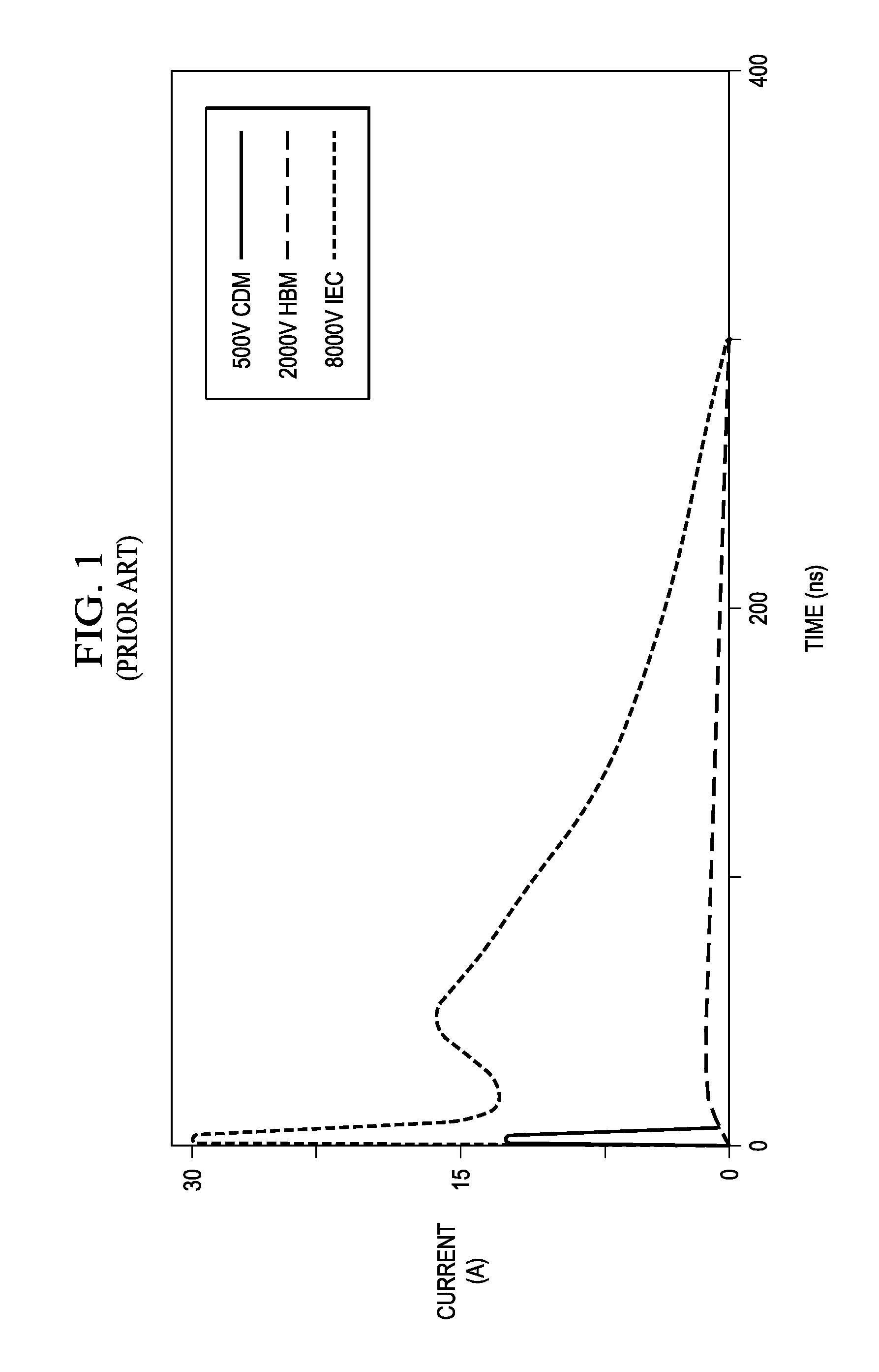
a technology of ic and thin film, applied in the field of electronic systems and semiconductor devices, can solve the problems of high stress current discharge in system-level esd (iec) events, inability to adapt to the structure, and inability to meet the requirements of device miniaturization,

Active Publication Date: 2008-11-13
TEXAS INSTR INC
View PDF5 Cites 32 Cited by
  • Summary
  • Abstract
  • Description
  • Claims
  • Application Information

AI Technical Summary

Benefits of technology

[0021]The thickened metal layers on the substrate top and bottom are etched to create terminals for the metal-filled through-holes. The terminals are distributed, for each device site, between usage for signal and power, and for ground. The selection of the signal and power terminals on the substrate bottom is performed so that the trace, to which each terminal is connected, overlaps with a trace on the opposite surface of the sheet, and that the opposite trace is connected to ground. As a consequence, an electrostatic overcharge that hits the signal / power terminal will readily initiate a local switching of the sheet material to conductor mode and thus bypass the overcharge to ground without giving the transient a chance to damage the corresponding signal / power terminal and the electronic component on the substrate top. This advantage provides protection against transients even for very fine pitch center-to-center of the terminals.

Problems solved by technology

The structural complexity, especially the cavities of the electrostatic discharge layer, does not lend itself to design fine-pitched device terminals; also, the overall protection thickness does not facilitate device miniaturization.
Further, the inherent resistance in the range of few hundred mΩ of the protection circuits makes the discharge of the high stress currents in the system-level ESD (IEC) events problematic.
In addition, the fabrication method in prior art is cumbersome and thus expensive; it does not lend itself to mass production and low cost.

Method used


Image

  • In package ESD protections of IC using a thin film polymer
  • In package ESD protections of IC using a thin film polymer
  • In package ESD protections of IC using a thin film polymer

Examples


Embodiment Construction

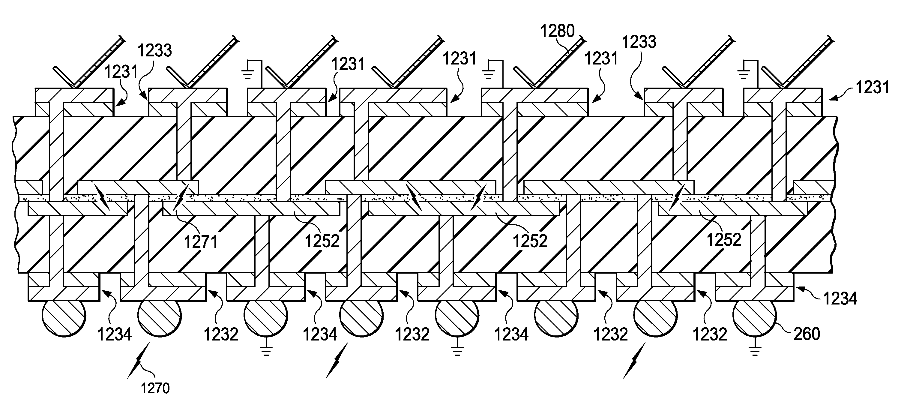
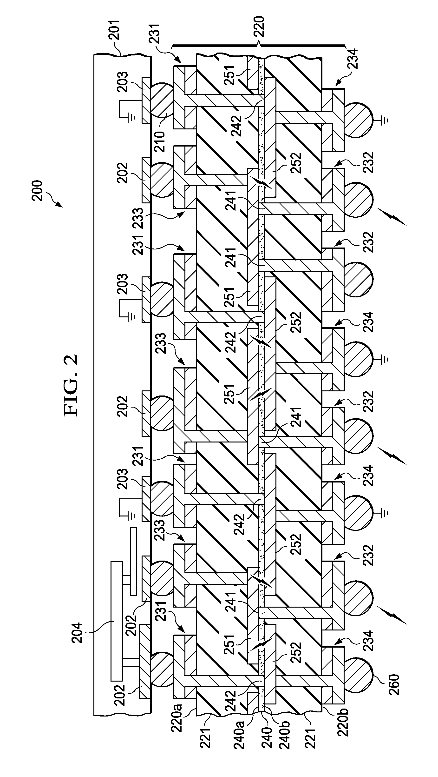
[0036]FIG. 2 illustrates a schematic cross section of an embodiment of the invention, which is an electronic device generally designated 200 with protection against transients. Device 100 includes an electronic component 201 connected by solder bodies 210 to a substrate 220. Component 201 may be a semiconductor chip, or may be another device in need for protection against electrostatic discharge, system level transients, cable discharge events, transient latch-ups, or any other electrostatic overcharge events. As FIG. 2 shows, chip 201 has metallic electrodes for external connections. According to their electrical function, the electrodes are grouped in sets: First electrodes 202 serve electrical signal and power, and second electrodes 203 serve electrical ground potential (or supply / ground; zero power being equivalent to ground). One of the first electrodes is schematically shown with its own protection device 204.

[0037]FIG. 2 also shows a substrate 220, onto which the component 20...


PUM

PropertyMeasurementUnit
thicknessaaaaaaaaaa
thicknessaaaaaaaaaa
electrical resistanceaaaaaaaaaa

Abstract

A packaged semiconductor device (200) with a substrate (220) having, sandwiched in an insulator (221), a flat sheet-like sieve member (240) made of a non-linear material switching from insulator to conductor mode at a preset voltage. Both member surfaces are free of indentations; the member is perforated by through-holes, which are grouped into a first set (241) and a second set (242). Metal traces (251) over one member surface are positioned across the first set through-holes (241); each trace is connected to a terminal on the substrate top and, through the hole, to a terminal on the substrate bottom. Analogous for metal traces (252) over the opposite member surface and second set through-holes (242). Traces (252) overlap with a portion of traces (252) to form the locations for the conductivity switches, creating local ultra-low resistance bypasses to ground for discharging overstress events.

Description

FIELD OF THE INVENTION[0001]The present invention is related in general to the field of electronic systems and semiconductor devices and more specifically to structure and method of local electrostatic discharge protection built into the package of the devices using a non-linear film.DESCRIPTION OF RELATED ART[0002]In the ongoing trend of scaling the silicon technologies towards the nanometer range, the ever-present challenge of protection against electrostatic discharge (ESD) and other destructive transient effects, such as cable discharge events, transient latch-ups, and electrostatic overcharge (EOS), has become even more difficult. The shrinking geometries of the integrated circuit (IC) reduce the intrinsic capability of the transistors to handle high ESD currents, and reduce the gate oxide breakdown voltage, but increase the metal resistance under ESD conditions.[0003]Additional ESD challenges are presented by the requirements of high performance / high speed circuits for low lea...

Claims


Application Information

Patent Timeline
Patent Type & Authority Applications(United States)
IPC IPC(8): H02H9/04H01H11/00
CPCH01L23/60H01L23/62H01L2224/16225Y10T29/49105H01L2924/15311H01L2924/13034H01L2924/00014H05K1/0259H05K2201/0738H01L2224/0557H01L2224/05573H01L2224/056H01L2224/05571H01L2224/0554H01L2224/05599H01L2224/0555H01L2224/0556
Inventor LEDUC, YVESMESSINA, NATHALIEDUVVURY, CHARVAKAWACHTLER, KURT P.
Owner TEXAS INSTR INC
Why Eureka
Try Eureka