Supercharge Your Innovation With Domain-Expert AI Agents!

Electromagnetic Shielding Device for an Infrared Receiver

Active Publication Date: 2008-11-20
YANG JIAXIANG
View PDF2 Cites 2 Cited by
  • Summary
  • Abstract
  • Description
  • Claims
  • Application Information

AI Technical Summary

Benefits of technology

[0003]The object of the present invention is to provide an electromagnetic shielding device for an infrared receiver, which is easier to manufacture, low-cost, high qualified ratio and suitable for mass production.
[0009]The electromagnetic shielding device according to the present invention has the advantages of being simple in structure, reasonable in design, easy to manufacture, low-cost, high qualified ratio and thus suitable for mass productivity. The electromagnetic shielding device improves the electromagnetic interference preventive capability of a semiconductor element, and thus significantly increases the sensibility and reliability of an infrared receiver.

Problems solved by technology

An infrared receiver is a fundamental device for realizing the remote control function of household electrical appliances, but the normal operation of the infrared receiver is influenced by external electromagnetic interference due to its high internal gain.

Method used


Image

  • Electromagnetic Shielding Device for an Infrared Receiver
  • Electromagnetic Shielding Device for an Infrared Receiver
  • Electromagnetic Shielding Device for an Infrared Receiver

Examples


first embodiment

The First Embodiment

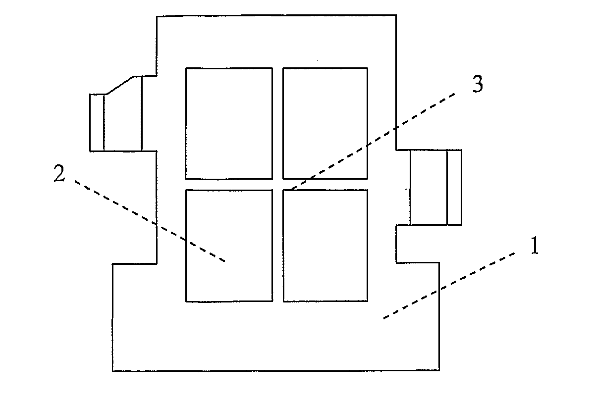
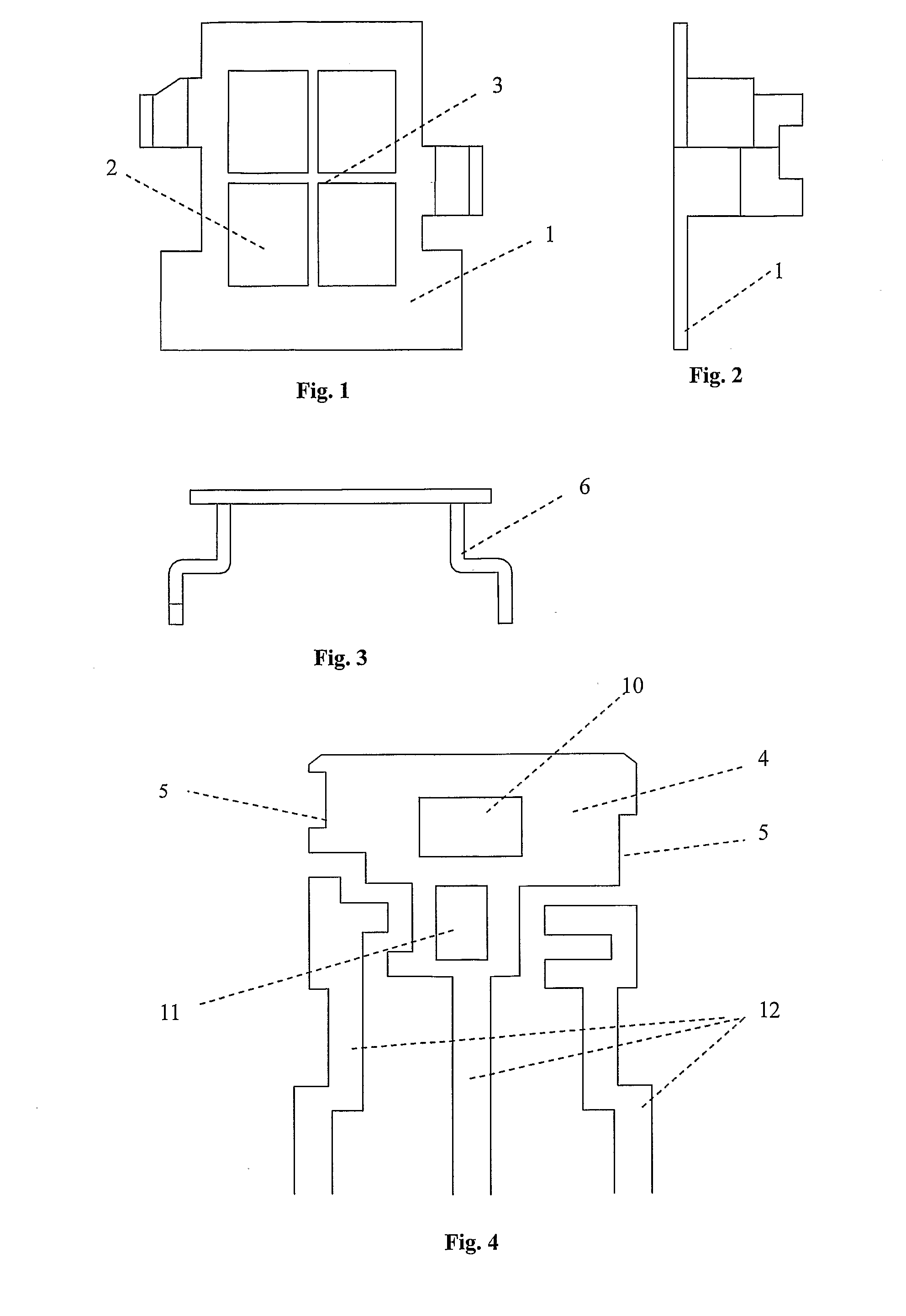
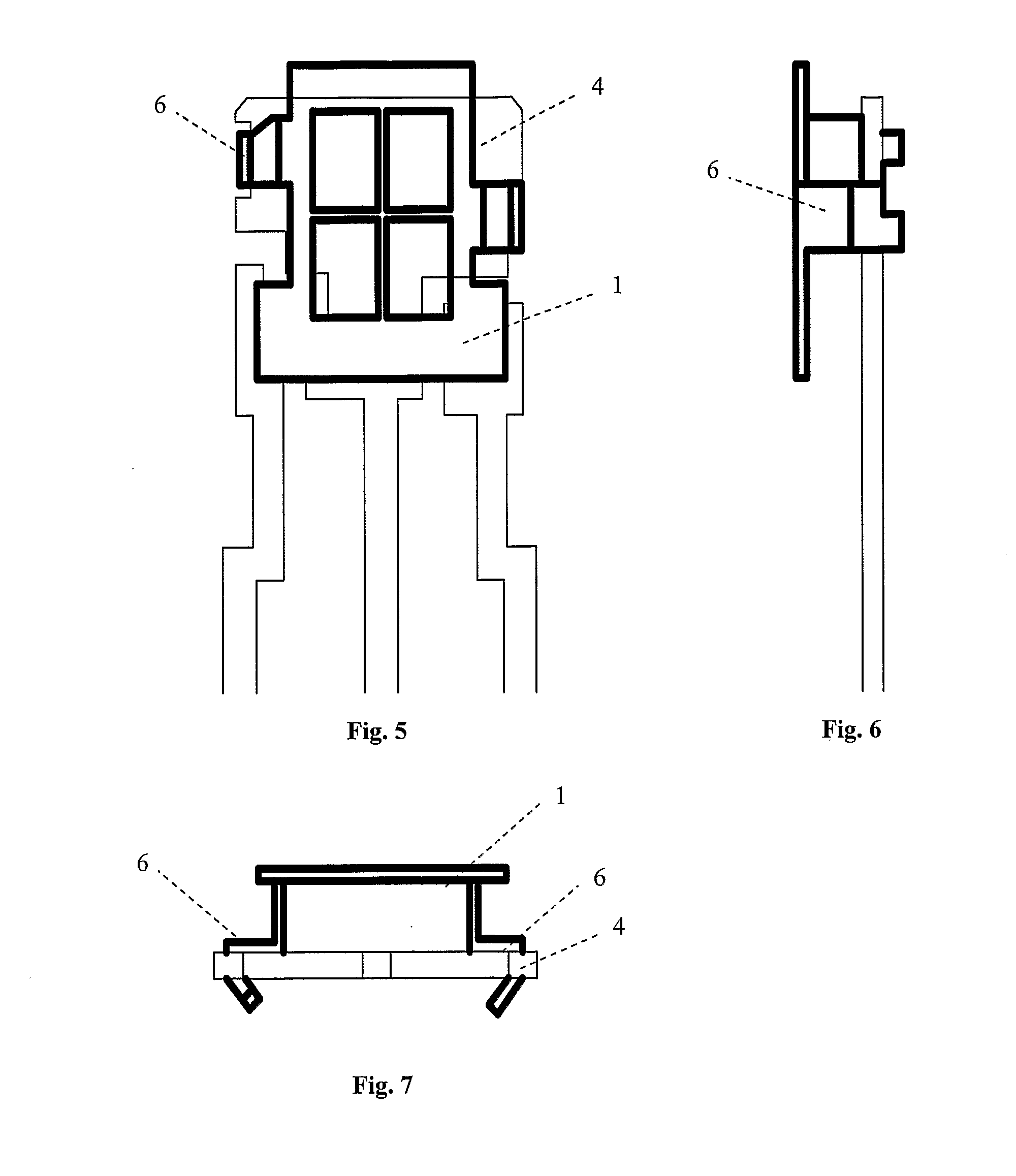
[0035]With reference to FIGS. 1 to 3, according to the first embodiment of the present invention, there is a window 2 in the electromagnetic shielding cover 1, and a shielding net 3 is provided in the window 2. The electromagnetic shielding cover 1 has a protruding tongue 6 in the bottom of each of its two sides respectively. The protruding tongues 6 have two bends of 90° respectively, and are in a trapezoid shape.

[0036]With reference to FIG. 4, a wiring frame 4 is formed with two positioning notches 5 on its both sides. A receiving diode chip 10 and an IC chip 11 are mounted in the wiring frame 4. Herein, the receiving diode chip 10 and the IC chip 11 are connected with functional circuits of the household electrical appliances, etc. via leads 12. The wiring frame 4 can be of pure metal, and can also be other types of wiring frames of copper-coated plate, metallized ceramic, and the like.

[0037]With reference to FIGS. 5 to 7, the two protruding tongues 6 of the e...

second embodiment

The Second Embodiment

[0042]With reference to FIGS. 8 to 10, according to the second embodiment of the present invention, there is a window 2 in the electromagnetic shielding cover 1, and a shielding net 3 is provided in the window 2. The electromagnetic shielding cover 1 has a protruding tongue 6 in the bottom of each of its two sides respectively. The protruding tongues 6 have no bends and are in a planar shape.

[0043]With reference to FIG. 11, the wiring frame 4 is formed with two positioning notches 5 on its both sides. A receiving diode chip and an IC chip (which are similar with those in the first embodiment and are not shown here) are mounted in the wiring frame 4. Herein, the receiving diode chip and the IC chip are connected with functional circuits of the household electrical appliances, etc. via leads 12. The wiring frame 4 can be of pure metal, and can also be other types of wiring frames of copper-coated plate, metallized ceramic, and the like.

[0044]With reference to FIGS...

third embodiment

The Third Embodiment

[0048]With reference to FIGS. 15 to 18, according to the third embodiment of the present invention, there is a window 2 in the metal electromagnetic shielding cover 1, and a shielding net 3 is provided in the window 2. The metal electromagnetic shielding cover 1 has an “n” shape protruding lugs in the bottom of its both sides respectively. The “n” shape protruding lugs branch into a long valvule and a short one. The long valvule 7 bends toward the short one to engage on the wiring frame 4. Besides, the metal electromagnetic shielding cover has in its bottom a tongue-shaped part 8.

[0049]With reference to FIG. 19, the wiring frame 4 is formed with two positioning notches 5 on its upper sides for fixing the “n” shape protruding lugs of the electromagnetic shielding cover 1. There is an “L” shape slot 9 in the center of the wiring frame 4, which engages with the tongue-shaped part 8 of the electromagnetic shielding cover 1 to position the electromagnetic shielding co...


PUM


Abstract

An electromagnetic shielding device in an infrared receiver comprises of a wiring frame (4) of metal and an electromagnetic shielding cover (1) of metal. There is a window (2) in the electromagnetic shielding cover (1), in which there is provided a shielding net (3). The electromagnetic shielding cover (1) has a protruding tongue (6) in the bottom of its both sides respectively and the protruding tongues (6) are bent downwards and entad to engage on the wiring frame (4), thus forming an electromagnetic shielding structure transparent to a chip inside. The electromagnetic shielding device of the present invention is simple in structure, reasonable in design, easy to manufacture, low-cost, high qualified ratio and thus suitable for mass productivity. The electromagnetic shielding device improves the electromagnetic interference preventive capability of a semiconductor element and thus increases the sensibility and reliability of an infrared receiver.

Description

FIELD OF THE INVENTION[0001]The present invention relates to a device for realizing electromagnetic shielding inside a semiconductor optoelectronic element, and more particularly to an electromagnetic shielding device inside an infrared receiver.BACKGROUND OF THE INVENTION[0002]An infrared receiver is a fundamental device for realizing the remote control function of household electrical appliances, but the normal operation of the infrared receiver is influenced by external electromagnetic interference due to its high internal gain. To overcome the adverse influence produced by the electromagnetic interference, it is necessary to provide an electromagnetic shielding device inside the infrared receiver. The present inventor has conducted a long-term research and experiment on the above issue, and has designed and proposed a novel technical solution. Based on this technical solution, the present inventor has filed a patent application in early 2003, which was granted on Apr. 7, 2004 un...

Claims


Application Information

Patent Timeline
IPC IPC(8): H01L23/552
CPCH01L27/14618H01L31/0203H04B10/69H05K9/0058H01L2924/0002H01L2924/00
Inventor YANG, JIAXIANG
Owner YANG JIAXIANG
Features
  • R&D
  • Intellectual Property
  • Life Sciences
  • Materials
  • Tech Scout
  • Unparalleled Data Quality
  • Higher Quality Content
  • 60% Fewer Hallucinations
Learn More