Method for Fabricating Array-Molded Package-On-Package

Inactive Publication Date: 2008-11-20
TEXAS INSTR INC
View PDF10 Cites 135 Cited by
  • Summary
  • Abstract
  • Description
  • Claims
  • Application Information

AI Technical Summary

Benefits of technology

[0005]The invention solves the problem by constructing one mold portion with contours so that the molded device will offer direct coupling with another device to form a package-on-package product. In addition, the new fabrication method is low-cost and simplified, and the products provide improved testability and thus yield. Using these contoured molds, stacking chips and packages will shorten the time-to-market of innovative products such as vertically integrated semiconductor systems, which utilize availa

Problems solved by technology

This simple approach, however, is no longer acceptable for the recent applications especially for hand-held wireless equipments, since these applications place new, stringent constraints on the size and volume of semiconductor components used for these applications.
This trend to reduce product thickness initiated an increasing tendency to have product warpage problems, especially in thin assemblies, cau

Method used


Image

  • Method for Fabricating Array-Molded Package-On-Package
  • Method for Fabricating Array-Molded Package-On-Package
  • Method for Fabricating Array-Molded Package-On-Package

Examples


Example

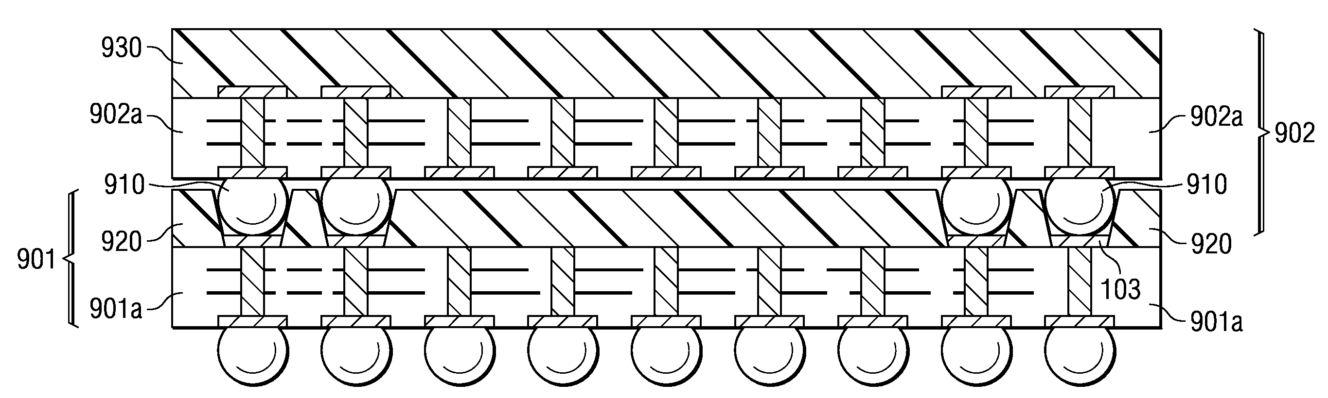
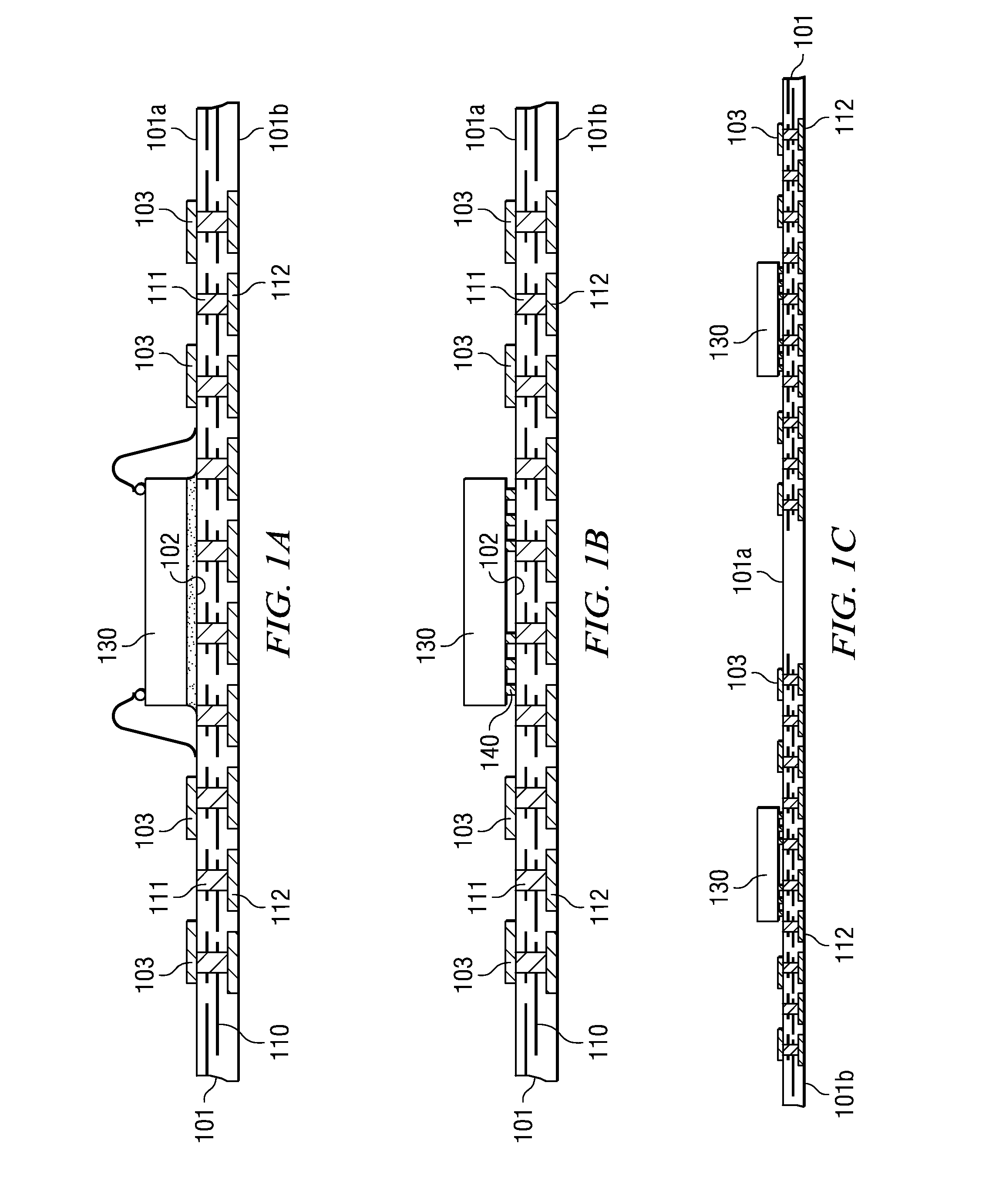
[0032]FIGS. 1A through 7 illustrate schematically the steps of one embodiment of the present invention, a method for array-molding semiconductor devices. The steps shown in FIGS. 1A and 1B show the assembly of a semiconductor chip on a substrate by wire bonding (FIG. 1A) and by flip-chip technology (FIG. 1B); FIG. 1C exemplifies a portion of an array of chips assembled by flip-chip. A sheet-like substrate 101 with insulating core (for example, plastic, glass-fiber reinforced, ceramic) is integral with two or more patterned layers of conductive lines and conductive vias (preferably copper) and contact pads in pad locations. Lines 110 do not reach beyond the boundaries of substrate 101. Substrate 101 has a first surface 101a and a second surface 101b, and a preferred thickness range from 0.2 to 0.5 mm. The first surface 101a includes chip assembly sites 102 and contact pads 103 in pad locations. The metal of the contact pads is preferably copper with a solderable surface (for example,...


PUM


Abstract

A method and apparatus for fabricating a semiconductor device are disclosed. The method attaches semiconductor chips (130) on a sheet-like insulating substrate (101) integral with two or more patterned layers of conductive lines and vias and with contact pads (103) in pad locations. A mold is provided, which has a top portion (210) with metal protrusions (202) at locations matching the pad locations. The protrusions are shaped as truncated cones of a height suitable to approach the pad metal surface in the closed mold cavity. The substrate and the chip are loaded onto the bottom mold portion (310); the mold is closed by clamping the top portion onto the bottom portion so that the protrusions are aligned with the contact pads, approaching the pad surface. After pressuring encapsulation compound into the cavity, the mold is opened; the encapsulated device has apertures to the pad locations. Any residual compound formed on the pads is removed by laser, plasma, or chemical to expose the metal surface.

Description

FIELD OF THE INVENTION[0001]The present invention is related in general to the field of semiconductor devices and processes and more specifically to the structure and fabrication method of low-profile, vertically integrated package-on-package integrated circuit assemblies.DESCRIPTION OF THE RELATED ART[0002]The thickness of today's semiconductor package-on-package products is the sum of the thicknesses of the semiconductor chips, electric interconnections, and encapsulations, which are used in the individual devices constituting the building-blocks of the products. This simple approach, however, is no longer acceptable for the recent applications especially for hand-held wireless equipments, since these applications place new, stringent constraints on the size and volume of semiconductor components used for these applications.[0003]Furthermore, while the market place renewed a push to shrink semiconductor devices both in two and in three dimensions, the miniaturization effort includ...

Claims


Application Information

Patent Timeline
IPC IPC(8): H01L23/48B05C13/00H01L21/58
CPCH01L21/561H01L21/565H01L23/49805H01L23/49816H01L24/81H01L24/97H01L25/105H01L2224/13144H01L2224/13147H01L2224/16H01L2224/32225H01L2224/48091H01L2224/48227H01L2224/48465H01L2224/48472H01L2224/73265H01L2224/81801H01L2224/97H01L2924/01029H01L2924/01032H01L2924/01046H01L2924/01079H01L2924/01082H01L2924/07802H01L2924/09701H01L2924/15311H01L2924/15331H01L2224/83H01L2224/85H01L2224/81H01L2924/00014H01L24/48H01L2924/01033H01L2924/01087H01L2924/014H01L2924/00H01L21/782H01L2924/3511H01L2924/00012H01L2225/1023H01L2225/1058H01L2224/16225H01L24/96H01L2924/181H01L2924/12042H01L24/73H01L2924/14H01L2224/0558H01L2224/05009H01L2224/0557H01L2224/05001H01L2224/05147H01L2224/05644H01L2224/05664H01L2924/1815H01L2224/05571H01L2224/05099H01L2224/45099H01L2224/45015H01L2924/207
Inventor GERBER, MARK A.WALTER, DAVID N.
Owner TEXAS INSTR INC
Why Eureka
Try Eureka