Electro-luminescence device and method of manufacturing electro-luminescence device
a technology of electroluminescence and electroluminescence device, which is applied in the direction of final product manufacturing, sustainable manufacturing/processing, semiconductor/solid-state device details, etc., can solve the problems of deterioration of display quality such as chromaticity change depending on viewing angle, difficulty in emitted one color, etc., and achieve high precision and improve the display quality of electro-luminescence device, without lowering reliability
- Summary
- Abstract
- Description
- Claims
- Application Information
AI Technical Summary
Benefits of technology
Problems solved by technology
Method used
Image

Examples
first embodiment
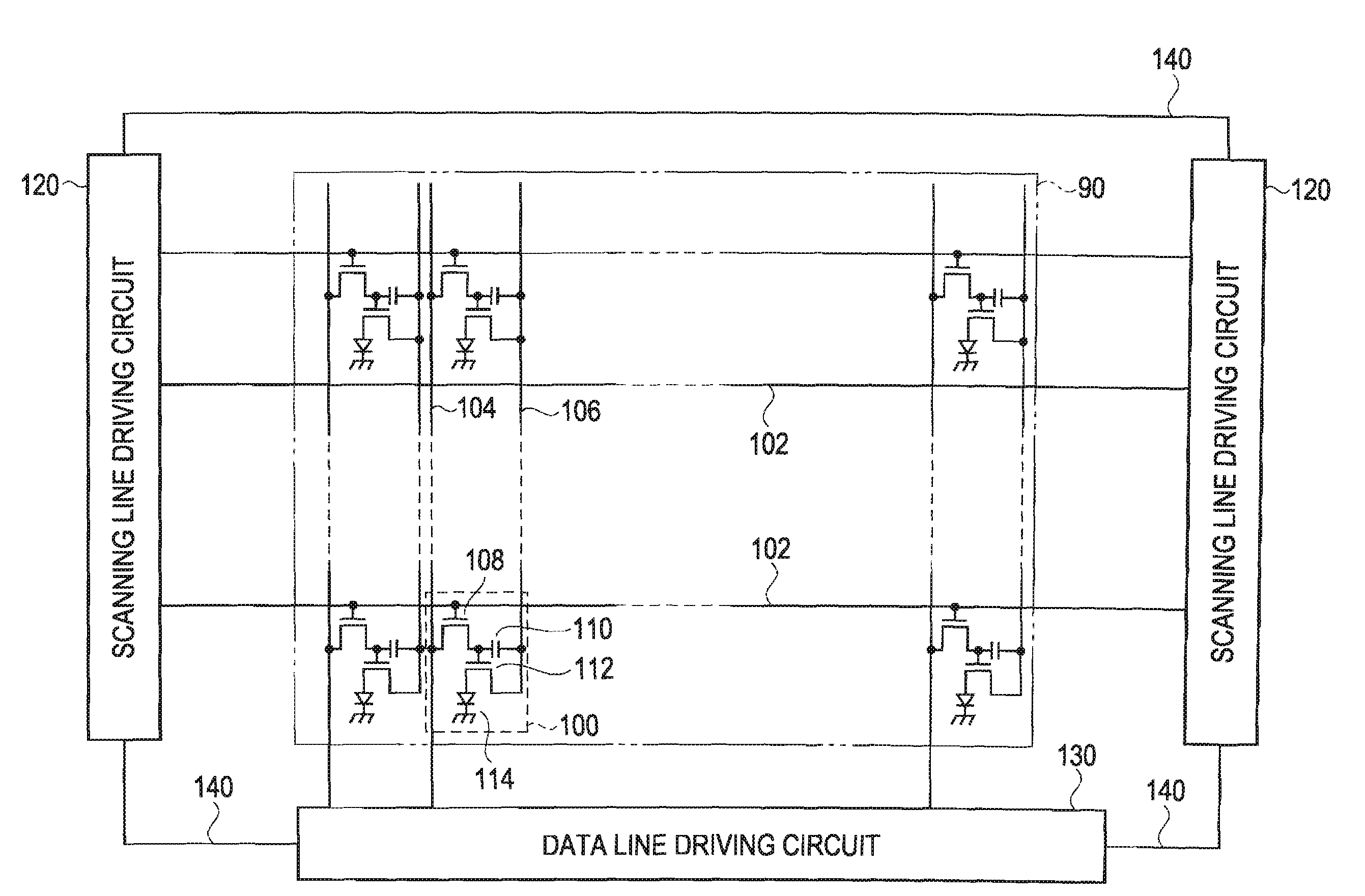
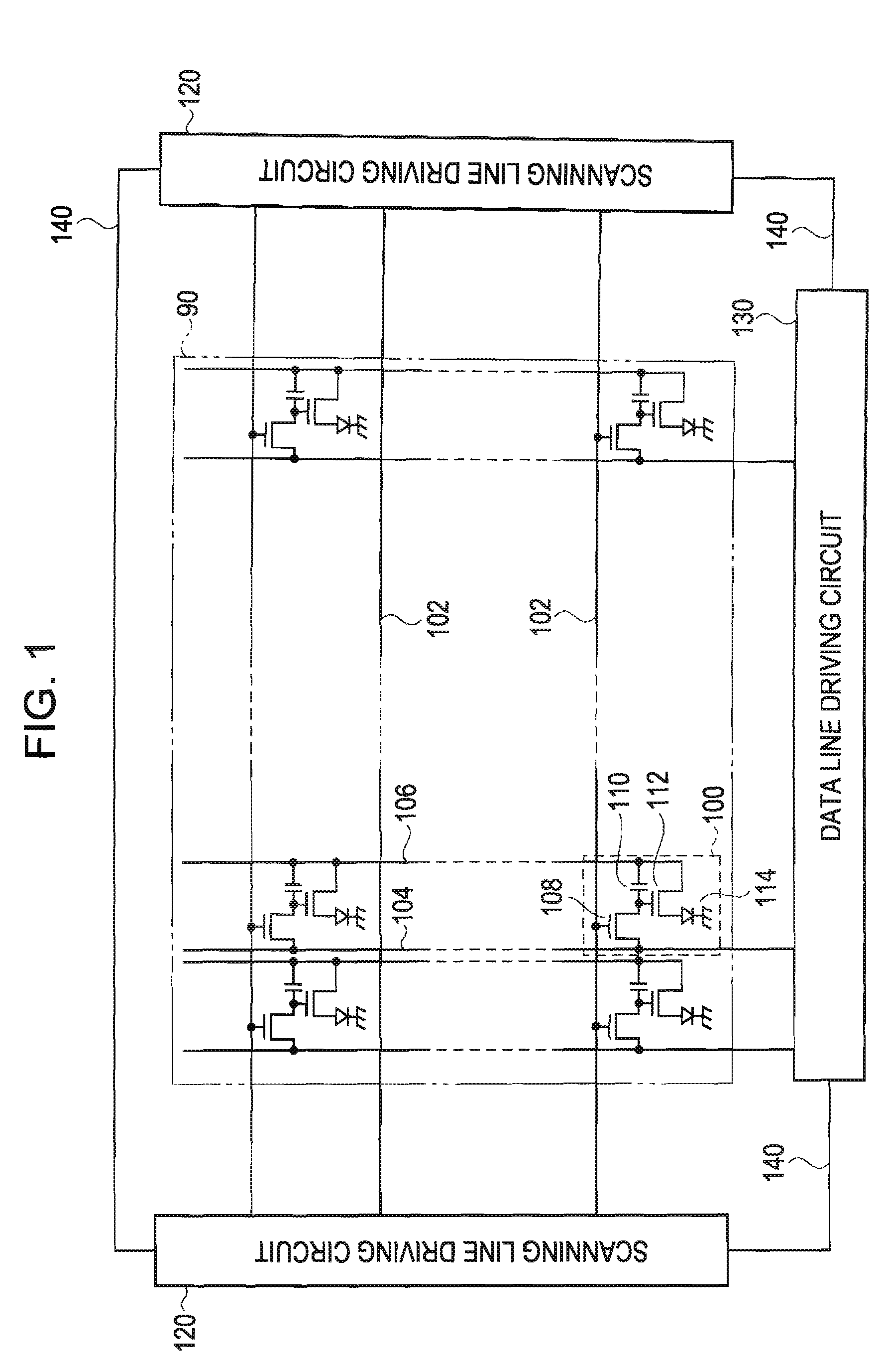
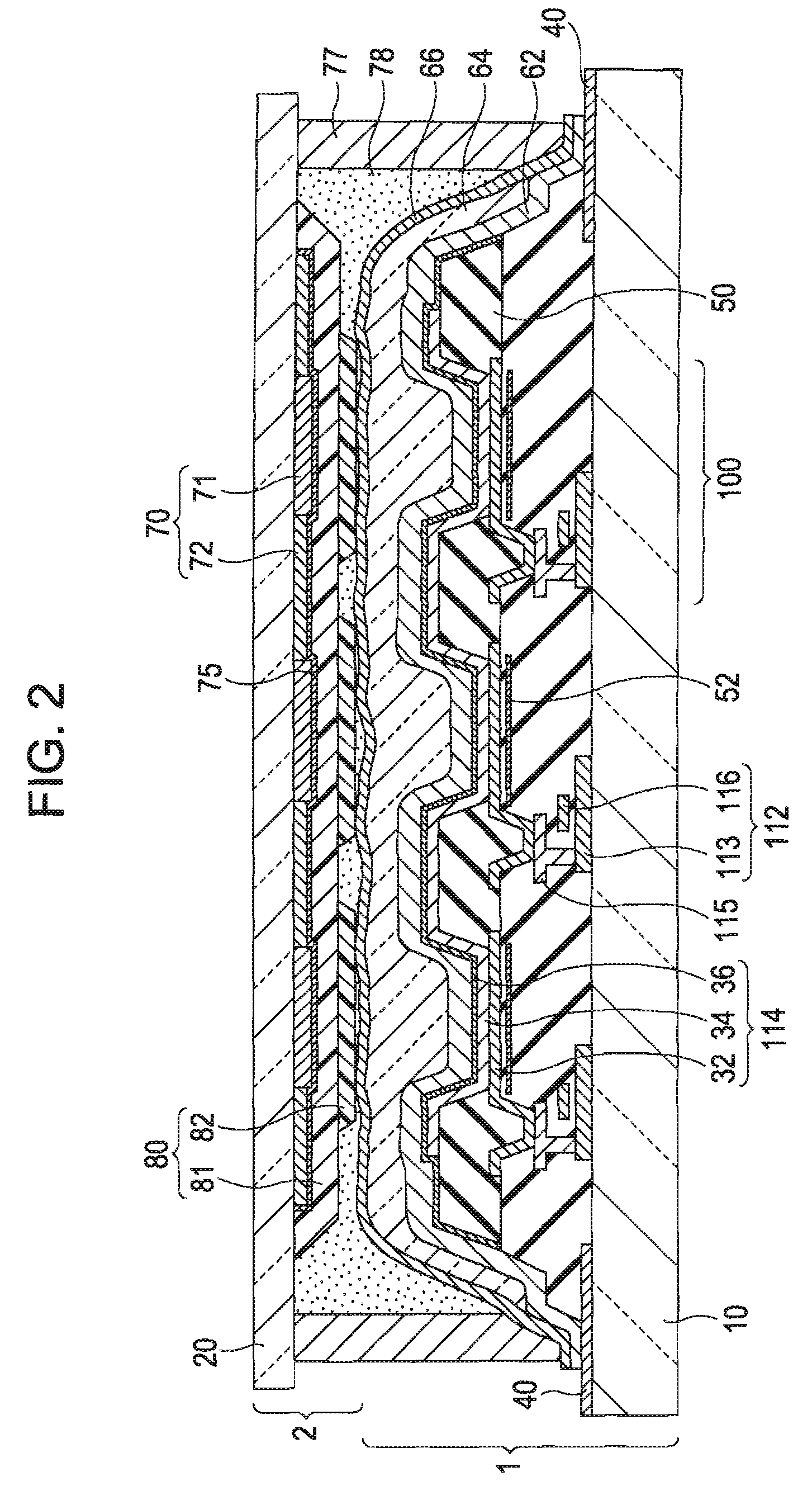
[0052]FIG. 2 is a schematic diagram showing the cross-section of a top emission type EL device according to a first embodiment of the invention. The figure is shown with primary focus on a color filter layer 70, a gap control layer 80, and a sealing layer which are needed for a description of the invention. Other elements such as a switching TFT 108, a holding capacitor 110, and the like that are not needed for the description of the invention are omitted or simplified in the figure.
[0053]The EL device according to this embodiment is formed by bonding a display base substrate 1 and a protection substrate 2 using a bonding layer to be described later. The display base substrate 1 includes a first substrate 10, a display body layer formed on the first substrate 10, and a sealing layer formed on the display body layer. Here, the display body layer represents a group of elements formed on the first substrate 10, that is, an aggregation of elements, wirings, and the like and includes a l...
second embodiment
[0078]FIGS. 4A to 4D are cross-section views showing a process of bonding the display base substrate 1 and the protection substrate 2 according to a second embodiment of the invention. In order to be adjusted for an actual bonding process, the embodiment shown in FIG. 2 is vertically reversed in this embodiments. In this embodiment, in order to represent interference between the gas barrier layer 66 and the second gap control layer 82, other constituent elements of the display base substrate 1 other than the gas barrier layer 66 are not show in the figure. In addition, to a constituent element of the protection substrate 2 common to that according to the first embodiment, a same reference numeral is attached, and a description thereof is omitted.
[0079]First, as shown in FIG. 4A, a peripheral sealing agent 77 is formed in the shape of a bank on the periphery of the protection substrate 2. The peripheral sealing agent 77 is supplied to the protection substrate 2 by using a needle disp...
third embodiment
[0089]FIG. 5 shows a protection substrate 2 according to a third embodiment of the invention. From this embodiment to an eighth embodiment of the invention, the gap control layer 80 is featured and the display base substrate 1 and the like are the same as those of the first and second embodiments, and thus only the protection substrate 2 is shown in the figure. In addition, to a constituent element common to this embodiment and the first embodiment, a same reference numeral is attached, and a description thereof is omitted.
[0090]The feature of the gap control layer 80 of the protection substrate 2 according to this embodiment is that the film thickness of the second gap control layer 82 is smaller than that of the first gap control layer 81. As described above, according to an embodiment of the invention, the first gap control layer 81 serves to maintain the gap has a constant value, and the second gap control layer 82 serves to absorb the pressure in the bonding process and suppres...
PUM
 Abstract
Description
Claims
Application Information
 - R&D
- Intellectual Property
- Life Sciences
- Materials
- Tech Scout
- Unparalleled Data Quality
- Higher Quality Content
- 60% Fewer Hallucinations
Browse by: Latest US Patents, China's latest patents, Technical Efficacy Thesaurus, Application Domain, Technology Topic, Popular Technical Reports.
© 2025 PatSnap. All rights reserved.Legal|Privacy policy|Modern Slavery Act Transparency Statement|Sitemap|About US| Contact US: help@patsnap.com