Contact barrier structure and manufacturing methods

a barrier structure and contact technology, applied in the direction of semiconductor devices, semiconductor/solid-state device details, electrical apparatus, etc., can solve the problems of increasing leakage current, increasing copper diffusion distance, and affecting the production efficiency of contact plugs, so as to reduce copper diffusion

Active Publication Date: 2008-11-27
TAIWAN SEMICON MFG CO LTD
View PDF5 Cites 26 Cited by
  • Summary
  • Abstract
  • Description
  • Claims
  • Application Information

AI Technical Summary

Benefits of technology

[0012]The advantageous features of the present invention include reduced copper diffusion into source / drain regions and the gate electrode of metal-oxide-semiconductor (MOS) devices.

Problems solved by technology

However, copper has greater diffusion distance.
This adversely increases the leakage currents, and may even cause device failure.
The high aspect ratio results in difficulties in the formation of contact barriers 12, which in turn causes bottom portions of the contact barriers to be discontinuous.
Copper thus adversely diffuses into the underlying source / drain regions and gate electrode.

Method used


Image

  • Contact barrier structure and manufacturing methods
  • Contact barrier structure and manufacturing methods
  • Contact barrier structure and manufacturing methods

Examples


Embodiment Construction

[0019]The making and using of the presently preferred embodiments are discussed in detail below. It should be appreciated, however, that the present invention provides many applicable inventive concepts that can be embodied in a wide variety of specific contexts. The specific embodiments discussed are merely illustrative of specific ways to make and use the invention, and do not limit the scope of the invention.

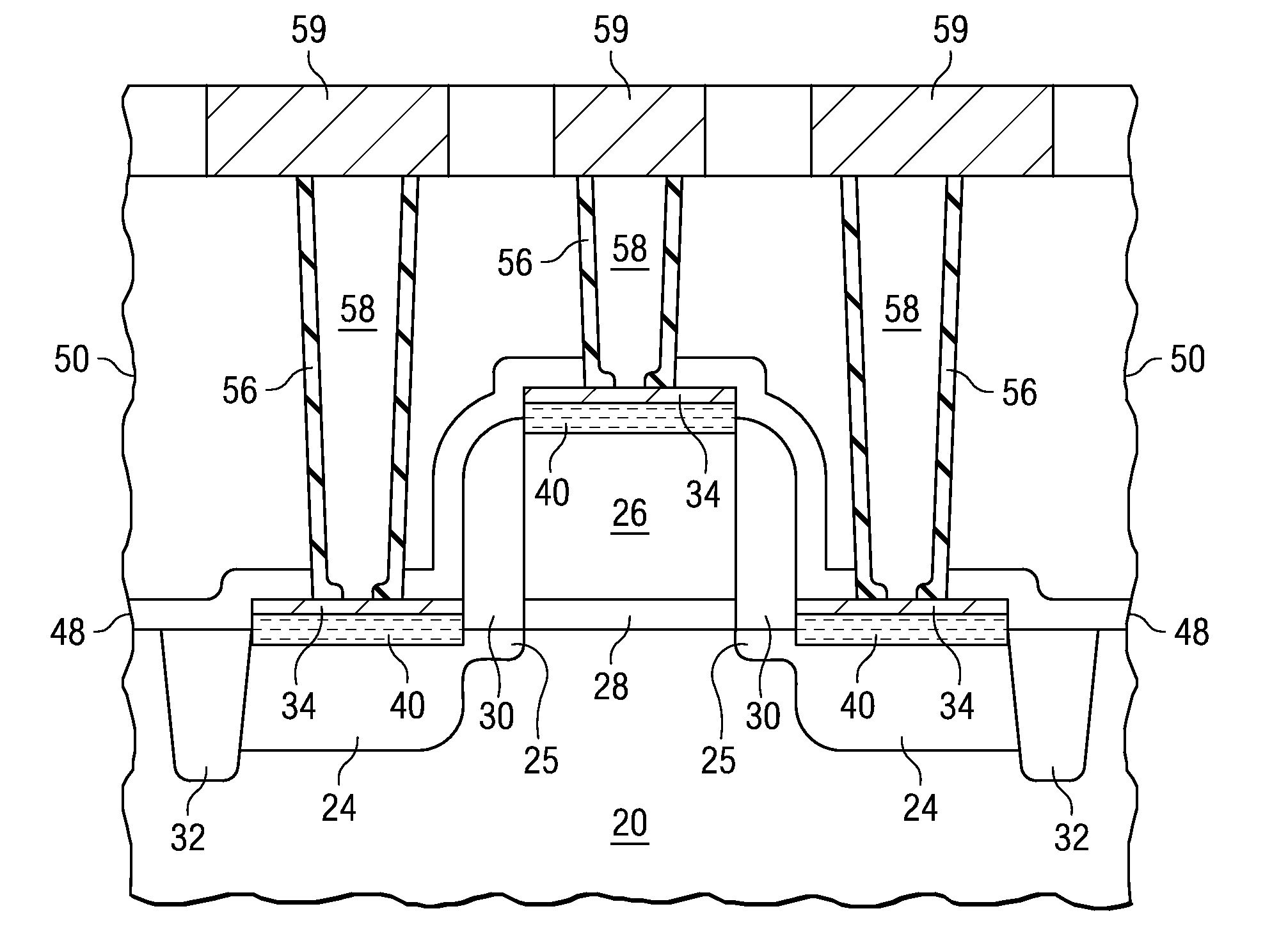
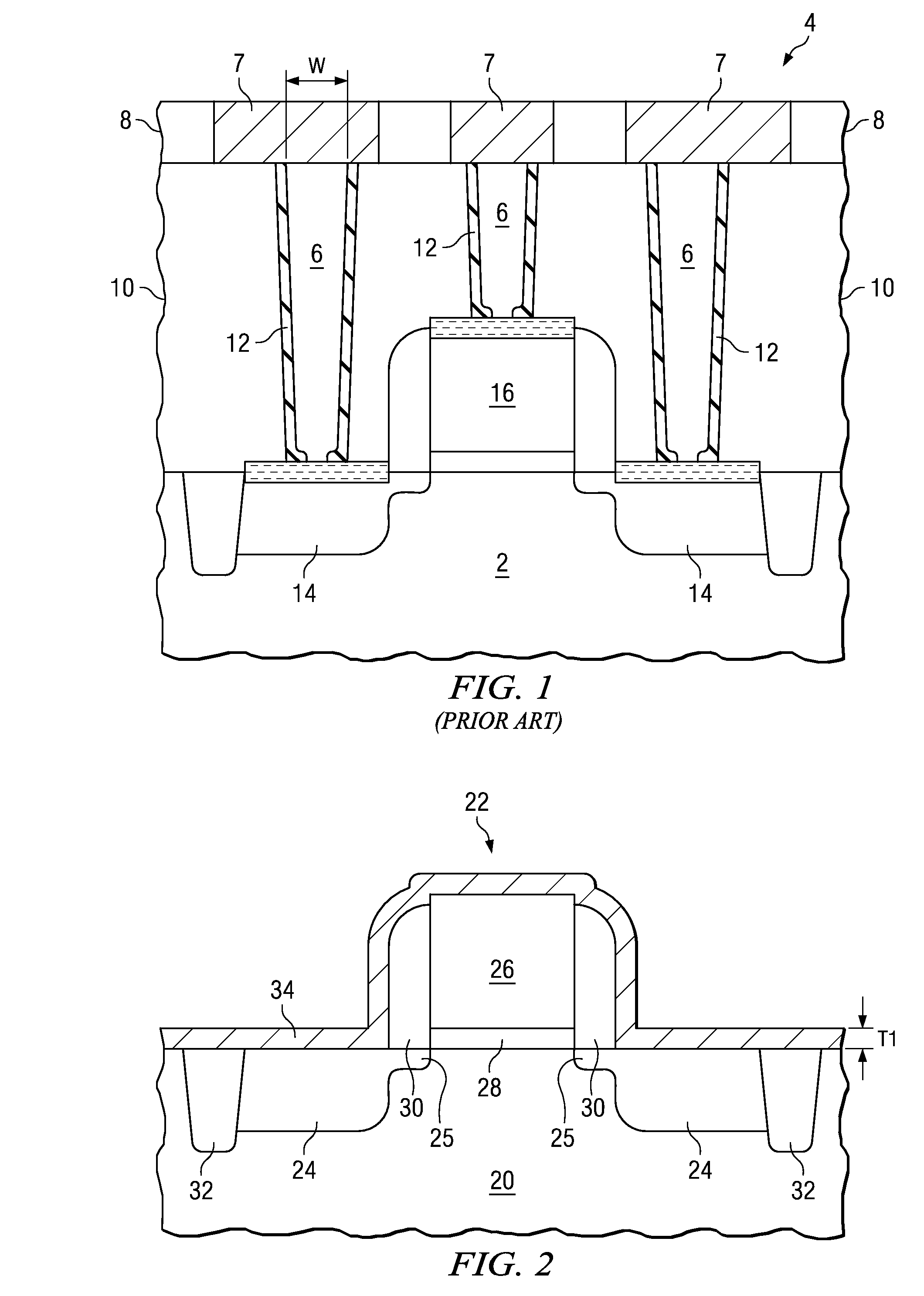
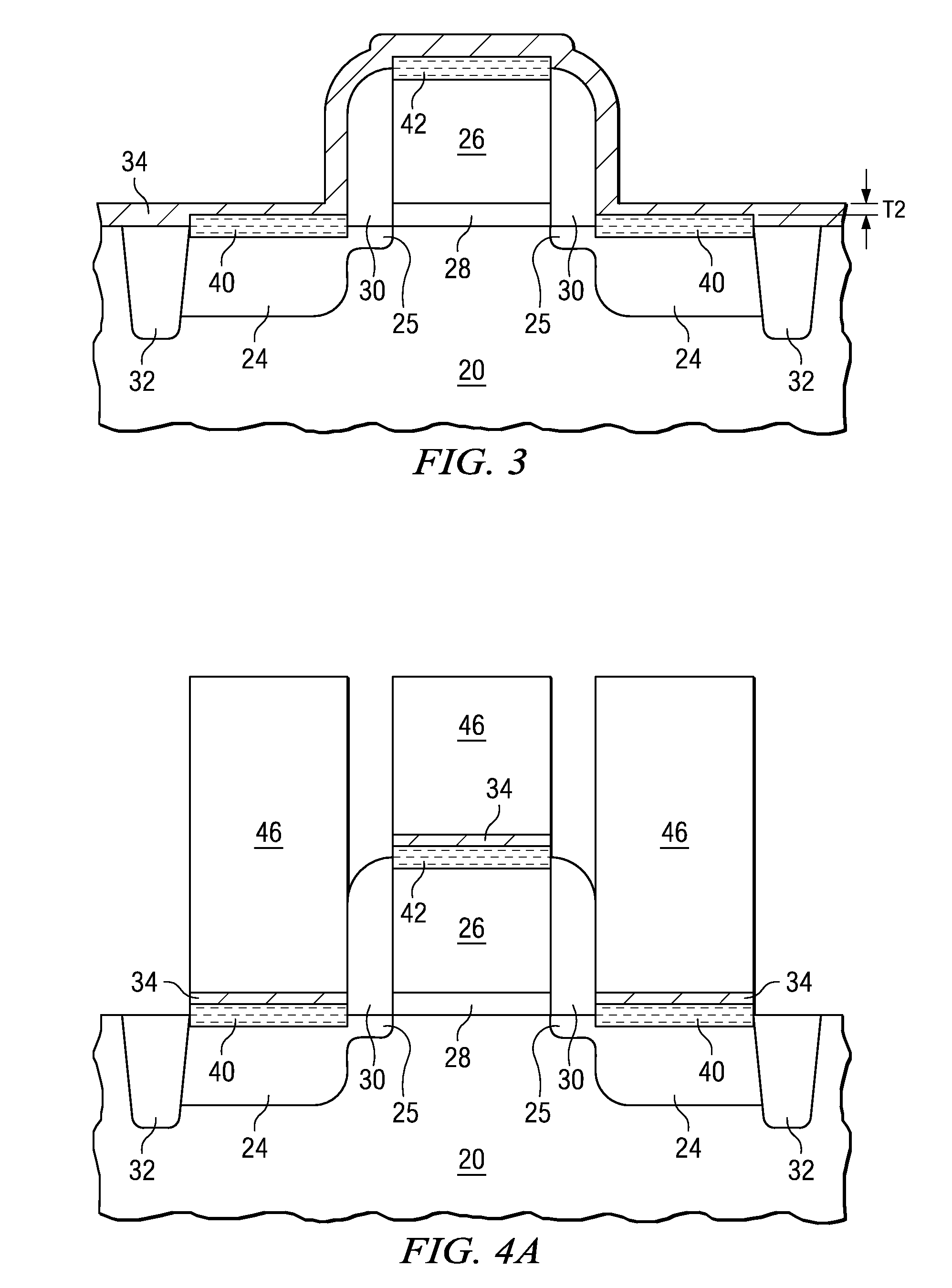
[0020]A novel contact structure is provided. The intermediate stages of manufacturing an embodiment of the present invention are illustrated. The variations of the embodiment are then discussed. Throughout the various views and illustrative embodiments of the present invention, like reference numbers are used to designate like elements.

[0021]FIGS. 2 though 6 illustrate cross-sectional views of a first embodiment of the present invention. Referring to FIG. 2, substrate 20 is provided. Substrate 20 is preferably a semiconductor substrate, which may include semiconductor materia...


PUM

PropertyMeasurementUnit
aspect ratioaaaaaaaaaa

Abstract

A semiconductor structure includes a semiconductor substrate; a gate dielectric over the semiconductor substrate; a gate electrode over the gate dielectric; a source / drain region adjacent the gate dielectric; a silicide region on the source / drain region; a metal layer on top of, and physical contacting, the silicide region; an inter-layer dielectric (ILD) over the metal layer; and a contact opening in the ILD. The metal layer is exposed through the contact opening. The metal layer further extends under the ILD. The semiconductor structure further includes a contact in the contact opening.

Description

TECHNICAL FIELD[0001]This invention relates generally to integrated circuits, and more particularly to the formation of contact plugs for connecting semiconductor devices and metallization layers.BACKGROUND[0002]In modern integrated circuits, semiconductor devices are formed on semiconductor substrates, and are connected through metallization layers. The metallization layers are connected to the semiconductor devices through contacts, also referred to as contact plugs. Also, external pads are connected to the semiconductor devices through the contacts.[0003]FIG. 1 illustrates conventional contacts for connecting the semiconductor devices to the metallization layers. Metal-oxide-semiconductor (MOS) device 4 is formed at the surface of semiconductor substrate 2. Inter-layer dielectric (ILD) 10 is formed over MOS device 4. Contacts 6 are formed in ILD 10 to connect source and drain regions 14 and gate 16 of MOS device 4 to metal lines 7, which are in metallization layer 8. Typically, t...

Claims


Application Information

Patent Timeline
Patent Type & Authority Applications(United States)
IPC IPC(8): H01L29/94H01L21/336
CPCH01L21/28518H01L21/76844H01L21/7685H01L29/665H01L29/66515H01L29/6659H01L29/7833H01L29/7848H01L23/485
Inventor WANG, CHING-YAKE, CHUNG-HULEE, WEN-CHIN
Owner TAIWAN SEMICON MFG CO LTD
Why Eureka
Try Eureka