
Shaping die for chip package leads

Inactive Publication Date: 2008-11-27
SEMICON MFG INT (SHANGHAI) CORP
View PDF15 Cites 0 Cited by
  • Summary
  • Abstract
  • Description
  • Claims
  • Application Information

AI Technical Summary

Benefits of technology

[0007]The invention provides a shaping die for chip package leads which improves the flatness of the shaped leads without damaging the package during the shaping procedure.
[0021]Compared with the prior art, the solutions mentioned above have the following advantages:
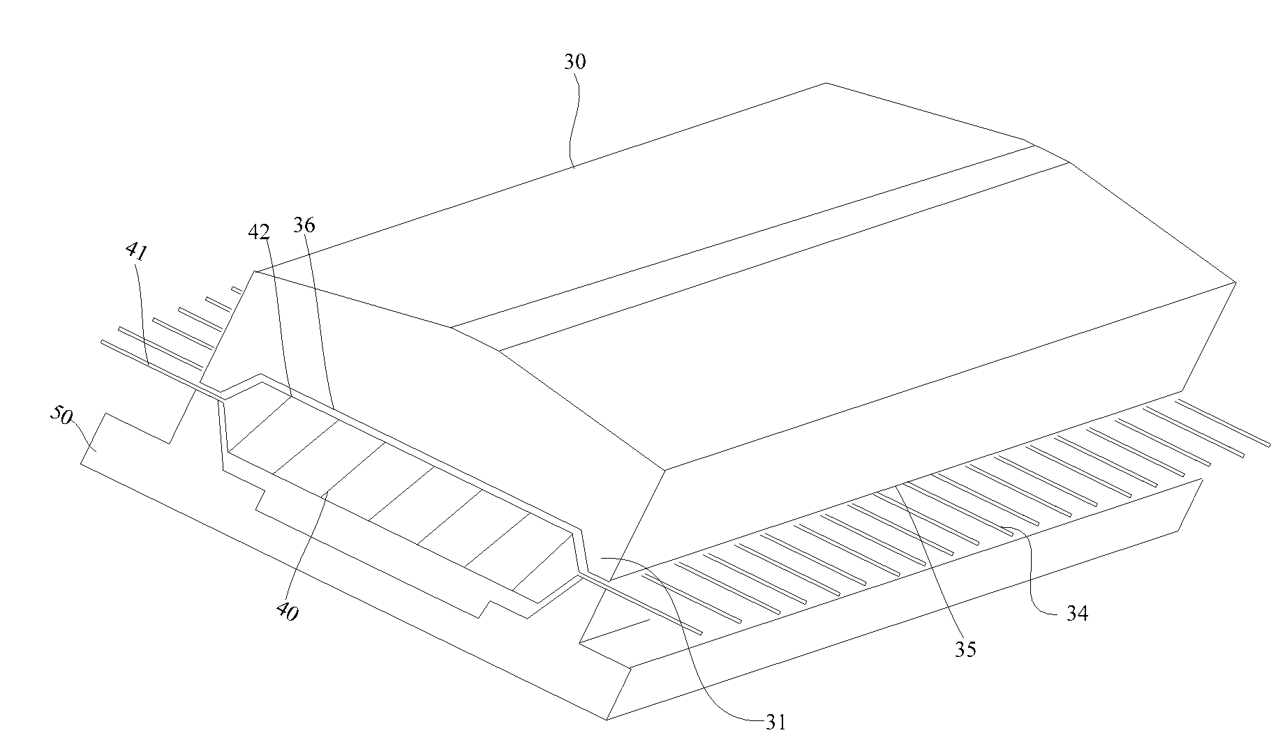
[0022]The shaping die for chip package leads is designed such that the contact portions of the lead pressing portions come into contact with the leads of the TSOP package when the shaping die holds the housing of the TSOP package and the contact portions only contact with a part of the leads of the TSOP package because of the warpage of the TSOP package. The depth of the groove can ensure that when the contact portions of the lead pressing portions come into contact with the surface of the part of the leads of the TSOP package, the inner surface of the groove will touch the surface of the upper housing of the TSOP package but will not apply force thereto so that the TSOP package will not be deformed. After shaping the leads by means of a punch head and removing the shaping die for chip package leads, the shaped leads of the TSOP package have better coplanarity, so that the TSOP package using the shaping die for chip package leads according to the invention will have well electrical connection property when it is surface mounted on the PCB or other substrate, and it will not cause broken circuit.
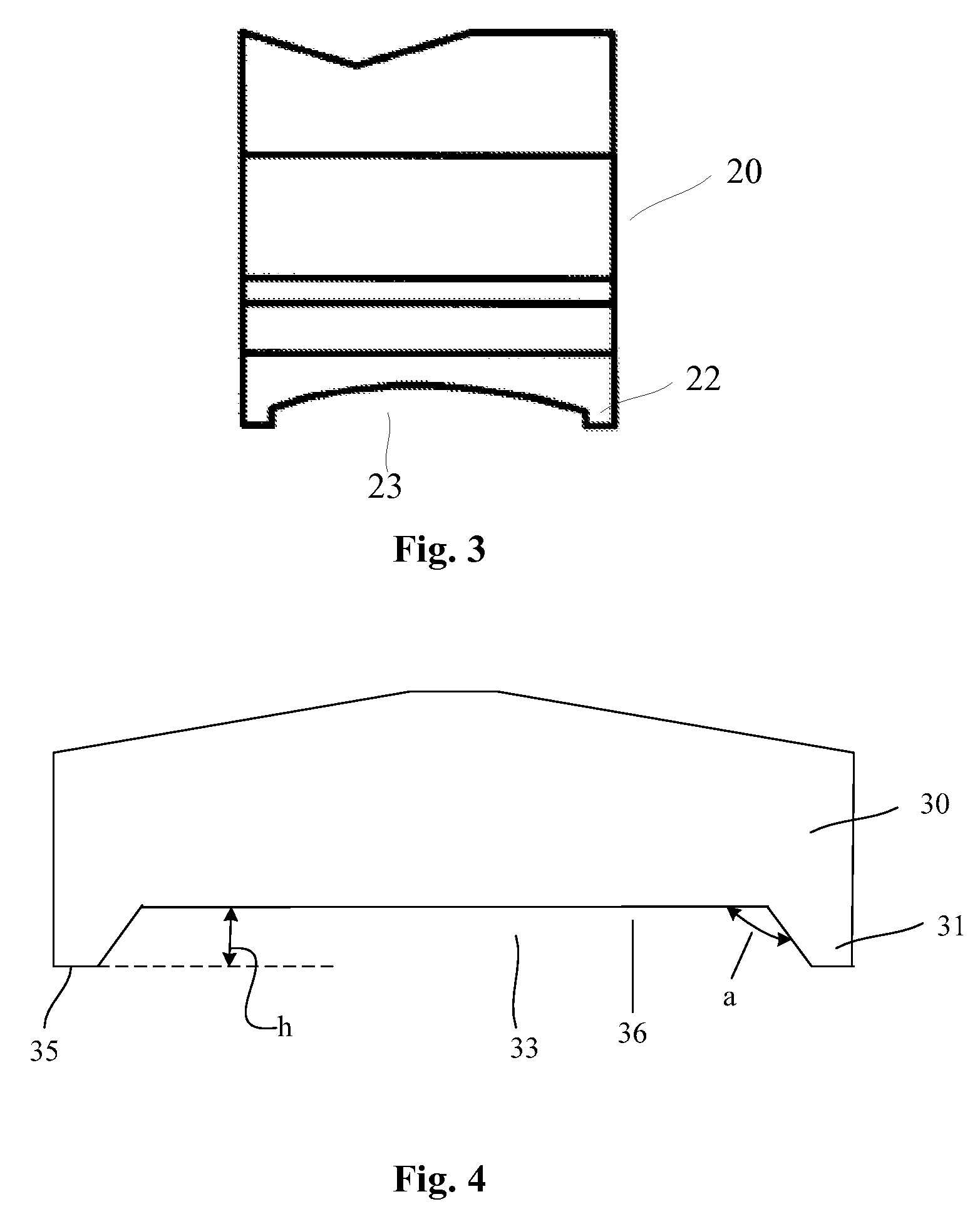
[0023]Furthermore, when the contact portions of the lead pressing portions come into contact with the surface of the part of the leads, the inner surface of the groove will touch the surface of the upper housing of the TSOP package with warpage, which fixes the TSOP package in a fixed state. When shaping the leads of the TSOP package in combination with the lower die and the punch head, the punch head punches the leads downwardly such that the roots of the leads produce a bounce force in the upward direction which brings the TSOP package to bounce upwardly. The depth h of the groove enables the surface of the upper housing of the warped TSOP package to contact with the inner surface of the groove, which prevents the upper housing of the TSOP package from warping upwardly. This further prevents the TSOP package from bouncing upwardly and hurting the TSOP chip, which reduces the damage to the TSOP package when shaping the TSOP package leads and helps to prolong the useful life of the chip.
[0024]The provision of the recess at the center of the groove can ensure that if there is a warpage in the short-side direction of the TSOP package the warpage will be compensated, so that the TSOP package will not be deformed when the shaping die for chip lead holds and fixes the chip.

Problems solved by technology

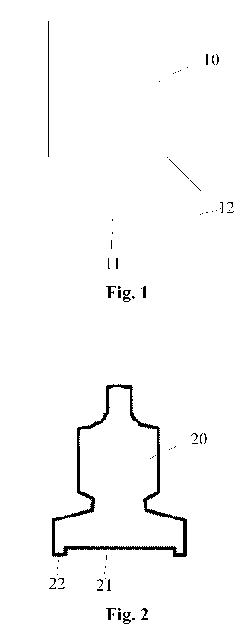
In order to achieve thin small outline package in the TSOP process, the Lead On Chip (LOC) structure is commonly adopted during the plastic package process, so that after being plastic packaged the upper and lower resin layers for plastic packaging of the chip have different thickness, which in turn causes the upper and lower resin layers of the chip to be contracted differently during the cooling procedure after being plastic packaged, resulting in the warpage of the formed package.
When removing the pressure applied to the TSOP package by the shaping die after the leads being shaped, the package will return to its warped state, which causes the coplanarity of the ends of leads contacted with other substrate or base plate (such as PCB) to be deteriorated.
However, when using the pressing block for shaping the leads to shape the TSOP package leads, the pressing block tends to hurt the package and make the package broken and damaged.

Method used


Image

  • Shaping die for chip package leads
  • Shaping die for chip package leads
  • Shaping die for chip package leads

Examples


first embodiment

[0038]FIGS. 4 and 5 are the front view and the left view of the shaping die for chip package leads according to the invention respectively.

[0039]The shaping die for chip package leads shown in FIGS. 4 and 5 comprises a base portion 30 and lead pressing portions 31 extending from the opposite sides of the base portion 30. The lead pressing portions 31 and the bottom surface of the base portion 30 define a groove 33 for holding the TSOP package. The lead pressing portions 31 have contact portions 35 contacting with the TSOP package leads.

[0040]The base portion 30 is generally made from alloy materials with higher hardness. The inner surface of the groove 33 is planar. The groove 33 is configured to hold the TSOP package when shaping the TSOP package leads. Thus, the shape of the groove 33 matches with that of the TSOP package and the lateral dimension of the groove 33 is slightly bigger than that of the TSOP package to facilitate the receiving and holding of the TSOP package. The dept...

second embodiment

[0049]FIGS. 8 and 9 are the front view and the left view of the shaping die for chip package leads according to the invention respectively.

[0050]The shaping die for chip package leads shown in FIGS. 8 and 9 comprises a base portion 30 and lead pressing portions 31 extending from the opposite sides of the base portion 30. The lead pressing portions 31 and the bottom surface of the base portion 30 define a groove 33 for holding the TSOP package. The lead pressing portions 31 have contact portions 35 contacting with the TSOP package leads.

[0051]The inner surface of the groove 33 is planar. The groove 33 is configured to hold the TSOP package when shaping the TSOP package leads. Thus, the shape of the groove 33 matches with that of the TSOP package and the lateral dimension of the groove 33 is slightly bigger than that of the TSOP package to facilitate the receiving and holding of the TSOP package. The depth h of the groove 33 corresponds to the maximum distance between the leads and th...


PUM

PropertyMeasurementUnit
Angleaaaaaaaaaa
Angleaaaaaaaaaa
Depthaaaaaaaaaa

Abstract

Disclosed herein is a shaping die for chip package leads including a base portion, on which lead pressing portions are provided, the lead pressing portions having contact portions contacting with TSOP package leads, a groove for holding the TSOP package being formed between the lead pressing portions, wherein the depth of the groove, which is the minimum distance between a location of the groove where the TSOP package is held and the contact portions of the lead pressing portions, corresponds to the maximum distance between the leads and the surface of the TSOP package held by the groove. The flatness of the shaped leads in the invention is improved and the package will not be damaged during the shaping procedure.

Description

CROSS-REFERENCES TO RELATED APPLICATIONS[0001]This application claims the benefit of Chinese Application No. 200710040985.0 filed on May 21, 2007.STATEMENT REGARDING FEDERALLY SPONSORED RESEARCH OR DEVELOPMENT FIELD[0002]Not applicable.BACKGROUND OF THE INVENTION[0003]The present invention relates to the field of semiconductor package, and more particularly to a shaping die for Thin Small Outline Package (TSOP) leads of the chip.[0004]TSOP is a kind of technology which involves forming pins around the chip and directly welding the pins of the packaged chip onto the surface of the Printed Circuit Board (PCB) by means of the Surface Mounting Technology (SMT). TSOP has been broadly applied since it has the advantages of high rate of finished products and lower cost and so on. In order to achieve thin small outline package in the TSOP process, the Lead On Chip (LOC) structure is commonly adopted during the plastic package process, so that after being plastic packaged the upper and lower...

Claims


Application Information

Patent Timeline
IPC IPC(8): B29C33/42
CPCH01L21/4842H01L2924/0002H01L2924/00
Inventor SHU, HAIBOPU, GUANGRONGTANG, ZHINENGLI, MIN
Owner SEMICON MFG INT (SHANGHAI) CORP
Learn More