Image Producing Methods and Image Producing Devices

a technology of image production and image, applied in the field of microlithography, can solve the problems of increasing stepper cost, reducing throughput, and complicated focusing system of giant projection lens, and achieve the effect of improving image resolution and simplifying equipment design

Inactive Publication Date: 2008-12-04
IVANOVA NATALIA VIKTOROVNA
View PDF6 Cites 6 Cited by
  • Summary
  • Abstract
  • Description
  • Claims
  • Application Information

AI Technical Summary

Benefits of technology

[0020]The technical result that might be obtained due to realization of proposed invention is significantly simplified technological process of high resolution patterns generation on the material sensitive to radiation used and simplified design of the equipment used, as well as improved image resolution during pattern generation. Besides, the use of near-field optical waveguides or field emission emitters allow avoiding the constrains related to the use of masks with diffraction limit and go to the approach that allows generating high resolution patterns of two-dimensional and three-dimensional structures without masks and practically without any diffraction distortions, this also provides the capability of getting smooth line edge and changing the intervals (gaps) between pattern elements with accuracy up to 0.01 nm, the distance between the radiators and material sensitive to radiation used with discrete up to 0.01 nanometer; this allows firstly, getting necessary accuracy at 1-50 nanometer distances, thus providing the work in the near field practically without diffraction limit and secondly, getting pre-defined change in the exposure spot diameter depending on the distance to radiation-sensitive material and consequently getting exact size of pattern element, for example the line of a pre-determined width, displacement to radiation-sensitive material and / or radiators in direction perpendicular to this line and exposure spots overlay for getting the pattern in the form of continuous line or any other shape, for example two-dimensional figure.

Problems solved by technology

Unfortunately, the resolution is increased at the sake of decreased focus depth ΔF, since ΔF=k2λ / A2, this consequently reduces the throughput and makes focusing system of giant projection lens very complicated, which again increases stepper cost.
Moreover, side effects limit the use of such lens aperture for maximum resolutions provided by the lens.
However, the cost of such stepper even at volume production would be according to experts estimate around 60 million US dollars and this will require according to most optimistic estimates 5-7 years to master mass production technology for microprocessors with characteristic 30 nm feature size.
As the leading manufacturers currently use wavelengths λ=193 nm and even less (in experiments!) it becomes evident how significant is the resolution limit caused by edge diffraction on the mask.
Therefore, existing projection devices used to generate patterns on a light-sensitive layer have essential drawbacks:1) significant difficulties of combining high resolution and focus depth in one device;2) as the wavelengths become shorter the design and technology of projection devices used to project patterns onto photoresist surface become far more complicated;3) as the wavelengths used for projection become shorter the optical system and technology of making mask object become extremely complicated;4) as the scale integration in the products grows the equipment and technology becomes extremely expensive;5) extremely low technological flexibility in the fabrication process and very costly re-adjustment;6) it is not possible in principle to make diversified manufacturing, i.e. fabrication of various integrated circuits on the same substrate with the same technological process
However, in the known method and apparatus for producing pre-defined image on entire substrate surface it is necessary to move radiation sensitive material to significant distances, which makes the apparatus design very complicated, degrades pattern resolution and increases the time of pattern generation on photoresist.
Besides, the known method and apparatus do not provide high pattern accuracy because the accuracy of exposure spots displacement over the surface of radiation-sensitive material is not adequate.

Method used


Image

  • Image Producing Methods and Image Producing Devices
  • Image Producing Methods and Image Producing Devices
  • Image Producing Methods and Image Producing Devices

Examples


Embodiment Construction

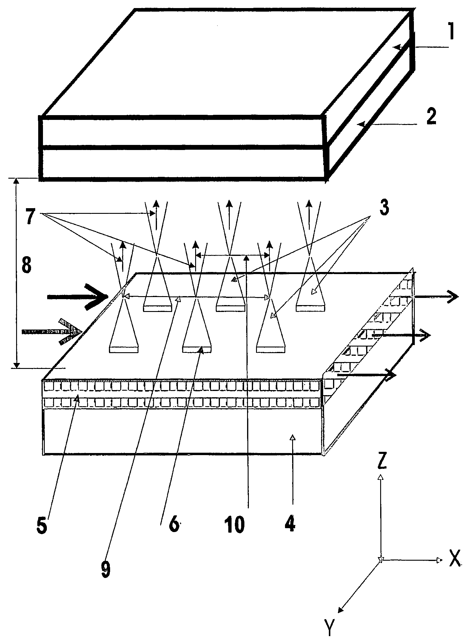
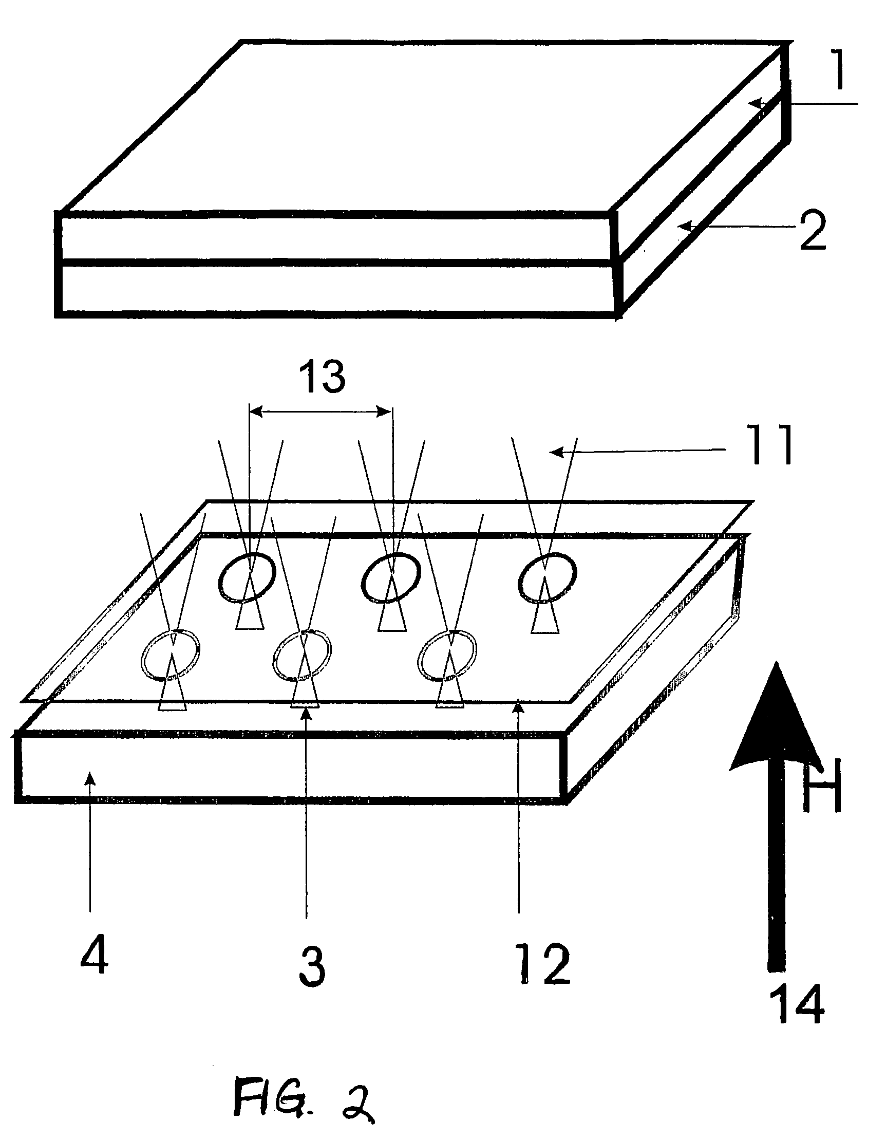
[0058]The apparatus (FIG. 1) for generating pattern on the material sensitive to used radiation, for example photoresist, includes the substrate 1 with photoresist layer coated thereon 2 and radiators array 3 located on a planar optical waveguide 5 and mounted on a unit 4 schematically shown on FIG. 1 designed for array mounting and moving. The radiator array shown in FIG. 1 as an example is realized as an array of waveguides connected to the source or sources of radiation (not shown). The waveguides are made as microcones of dielectric or semiconductor material transparent for used radiation and are coated with the layer reflecting this radiation; actually they are the near-field optical waveguides. They are located on the surface of planar waveguide 5, bringing radiation to the basis of near-field waveguides being microcones.

[0059]On the basis of microcones individually switched devices 6 realized for example as the gates regulating radiation entrance to microcones may be placed. ...


PUM

PropertyMeasurementUnit
diameteraaaaaaaaaa
diameteraaaaaaaaaa
distanceaaaaaaaaaa

Abstract

The invention relates to microlithography and can be used, for instance for producing integrated circuits or structures having a sub-micron resolution. An image is produced with the aid of the stepped displacement, including continuous displacement of the radiator matrix(es) and/or a material sensitive to a used radiation at a step which is less than d. The diameter of the radiation flux at the output of each radiator is less than 100 nm. The sizes of the radiator matrixes can be equal to or greater than an image size. The displacements are carried out at distances which are equal or less than a maximum center-to-center distance of two adjacent radiators. A matrix of waveguides which are connected to at least one radiation source and made of fibre-optic waveguides having thinned ends or embodied in the form of microcones made of a material which is transparent for the used radiation is used as the radiator matrix. An emissive emitter matrix can also be used in the form of said radiator matrix. Said invention makes it possible to radically simplify a technological process for producing high-resolution images and used equipment

Description

FIELD OF THE INVENTION[0001]The invention relates generally to microlithography, in particular to photolithography and can be industrially realized for example in the fabrication of integrated circuits or structures having pre-programmed submicron topography.BACKGROUND OF THE INVENTION[0002]The creation of integrated circuits with characteristic line width of 0.1-0.01 micron is an important and promising direction in the development of up-to-date microelectronics. The high-precision technology (with submicron and micron tolerances) of making precision shapes with three-dimensional topography can find industrial application for example in mass production of microrobotic parts, high resolution elements in diffraction and Fresnel optics and in other technological areas where it is required to obtain three-dimensional image with pre-determined depth and high resolution structures in the functional layer of a device, for example in the production of printing plates used for making bankno...

Claims


Application Information

Patent Timeline
Patent Type & Authority Applications(United States)
IPC IPC(8): G21K5/00G03C5/00G03F7/20
CPCG03F7/2057G03F7/2059G03F7/2065G03F7/7035G03F7/70358G03F7/70383G03F7/70391G03F7/70466G03F7/70475
Inventor IVANOVA, NATALIA VIKTOROVNA
Owner IVANOVA NATALIA VIKTOROVNA
Why Eureka
Try Eureka