Filament lamp and light-irradiation-type heat treatment device

a technology of heat treatment device and filament lamp, which is applied in the direction of gas-filled discharge tube, transit-time tube, electrical heating fuel, etc., can solve the problems of affecting the temperature of semiconductor wafer, and affecting the quality of semiconductor wafers

Inactive Publication Date: 2008-12-04
USHIO DENKI KK
View PDF13 Cites 12 Cited by
  • Summary
  • Abstract
  • Description
  • Claims
  • Application Information

AI Technical Summary

Benefits of technology

[0031]In view of the problem described above, the purpose of the present invention is to provide a filament lamp that assures insulation between a filament and the leads that surround that filament, and between leads in the vicinity of the filaments, so that unwanted discharge will not occur, and one in which there is no likelihood that unwanted light will be emitted. Another purpose of the present invention is to provide light-irradiation-type heat treatment device in which variations are not liable to occur during heat treatment of the workpiece to be treated.
[0045]Using the invention of the first aspect, advantageously, there is no likelihood of unwanted discharge between a filament and leads that are nearby in the direction perpendicular to the tube axis of the light emitting tube, and because the heat of the insulating wall is transferred to the light emitting tube and released to the air, the insulating tube does not reach a high temperature as in filament lamps of the related art, and so there is no likelihood that unwanted light other than from the filaments will be emitted. Moreover, the leads are located in lead accommodation spaces where they will not short circuit each other, and so it is possible to suppress unwanted discharge between adjacent leads. Advantageously, there is no likelihood that leads will melt through while the filament lamp is lit, and the filament lamp can be lit in a stable manner over a long period of time.
[0047]Using the invention of the fourth aspect, leads can be reliably positioned in the desired positions, so that movement of the leads in the circumferential direction is regulated, even with repeated thermal expansion and contraction of the leads, and the leads do not depart from their initial positions. Moreover, because non-machining methods such as drawing or injection molding can be adopted, damage to light emitting tubes during manufacture of the filament lamps can be avoided and productivity can be increased.
[0048]Using the invention of the fifth aspect, light emitted by the filament is emitted without attenuation by the insulating wall, and so the desired heat treatment can be conducted without an excessive use of power in the filament.
[0049]Using the of the sixth aspect, light emitted by the filaments is not attenuated by the insulating wall, and so the desired heat treatment can be conducted without an excessive use of power in the filament. Moreover, the operation of passing the leads through the openings formed in the insulating wall and pulling them outward from the insulating wall during manufacture of the filament lamp can be facilitated by inserting the filaments into the inner tube.
[0050]Using the invention of the seventh and eighth aspects, thermal conduction from the insulating wall to the light emitting tube is promoted, and so it is possible to more reliably keep the insulating wall from reaching a high temperature and there is no likelihood of the emission of unwanted light other than from the filaments. In particular, the inner surface of the light emitting tube and the insulating wall are fused together along the tube axis of the light emitting tube, and so it is possible to increase the area of fusion of the light emitting tube and the inner wall and further encourage thermal conduction from the insulating wall to the light emitting tube. Moreover, even if the insulating wall reaches a higher temperature than the light emitting tube while the filament lamp is lit and the insulating wall expands more than the light emitting tube in the direction of the tube axis of the light emitting tube, the shearing force that works between the light emitting tube and the insulating wall is dispersed, and so there is no likelihood of damage to the fused area.

Problems solved by technology

When the workpiece to be treated is, for example, a semiconductor wafer (e.g., a silicon wafer), if there is unevenness of the temperature distribution of the semiconductor wafer when it is heated to a temperature of 1050° C. or higher a phenomenon called “slip”, in which crystal transition defects arise and quality declines, is liable to occur in the semiconductor wafer.
Even in the event that the light irradiation is done so that the degree of irradiation is uniform for semiconductor wafers that have the same physical characteristics across the entire surface of the semiconductor wafer, the temperature of the semiconductor wafer will not be uniform.
It has been learned, however, that the problem described below may occur in the conventional heat treatment device described above.
Therefore, there is the problem of an undesirable temperature distribution in the treatment temperature of the workpiece 202 to be treated, and it becomes difficult to apply the desired physical properties to the workpiece 202 to be treated.
Nevertheless, in the event that the special regions do not have central symmetry with respect to the center of the semiconductor wafer, it is not possible to solve the problem described above properly because heat treatment is done by rotating the semiconductor wafer.
Moreover, it is thought that the following problems could occur if this heat treatment device 300 were actually used.
When the filament lamps were lit, however, it was learned that the problems explained below occurred because the insulating tubes absorbed light emitted by the filaments and reached high temperatures.
In these filament lamps, however, the insulating tubes are located within the light emitting tube, separated from the inner surface of the light emitting tube; and because there is no way to avoid a temperature rise by the insulating tubes, it is not possible to suppress the light emitted by the insulation tubes that have reached a high temperature.
Moreover, the irradiation intensity of the light emitted by these insulating tubes varies, depending on the temperature of the insulating tubes, and is also affected by various factors such as the distance between the insulating tube and filaments in proximity to the insulating tube, the thickness of the insulating tube, and the amount of power used for powering the filaments.
It is very difficult, therefore, to control uniformly the intensity of light emitted by the insulating tubes.
It was not possible, therefore, to obtain the desired treatment characteristics.
Nevertheless, if the insulating tubes are removed, putting the leads in the light emitting tube in a such an arrangement, the presence of numerous filament assemblies within the light emitting tube is liable to cause undesired discharge between filaments and the leads placed in the vicinity of the filaments, and between nearby leads among the multiple leads that surround a filament, which may result in the filament lamp becoming unusable because the leads can melt through.
However, when filament lamps are arranged with parallel tube axes, increasing the inside diameter of the light emitting tube would increase the separation between adjacent filaments in the direction perpendicular to the tube axes, which is liable to lead to deterioration of the distribution of illuminance on the workpiece to be treated.
That method would also increase the size of the light-irradiation-type heat-treatment equipment if the desired number of filament lamps were included, and so in practical terms it cannot be adopted.

Method used


Image

  • Filament lamp and light-irradiation-type heat treatment device
  • Filament lamp and light-irradiation-type heat treatment device
  • Filament lamp and light-irradiation-type heat treatment device

Examples


first embodiment

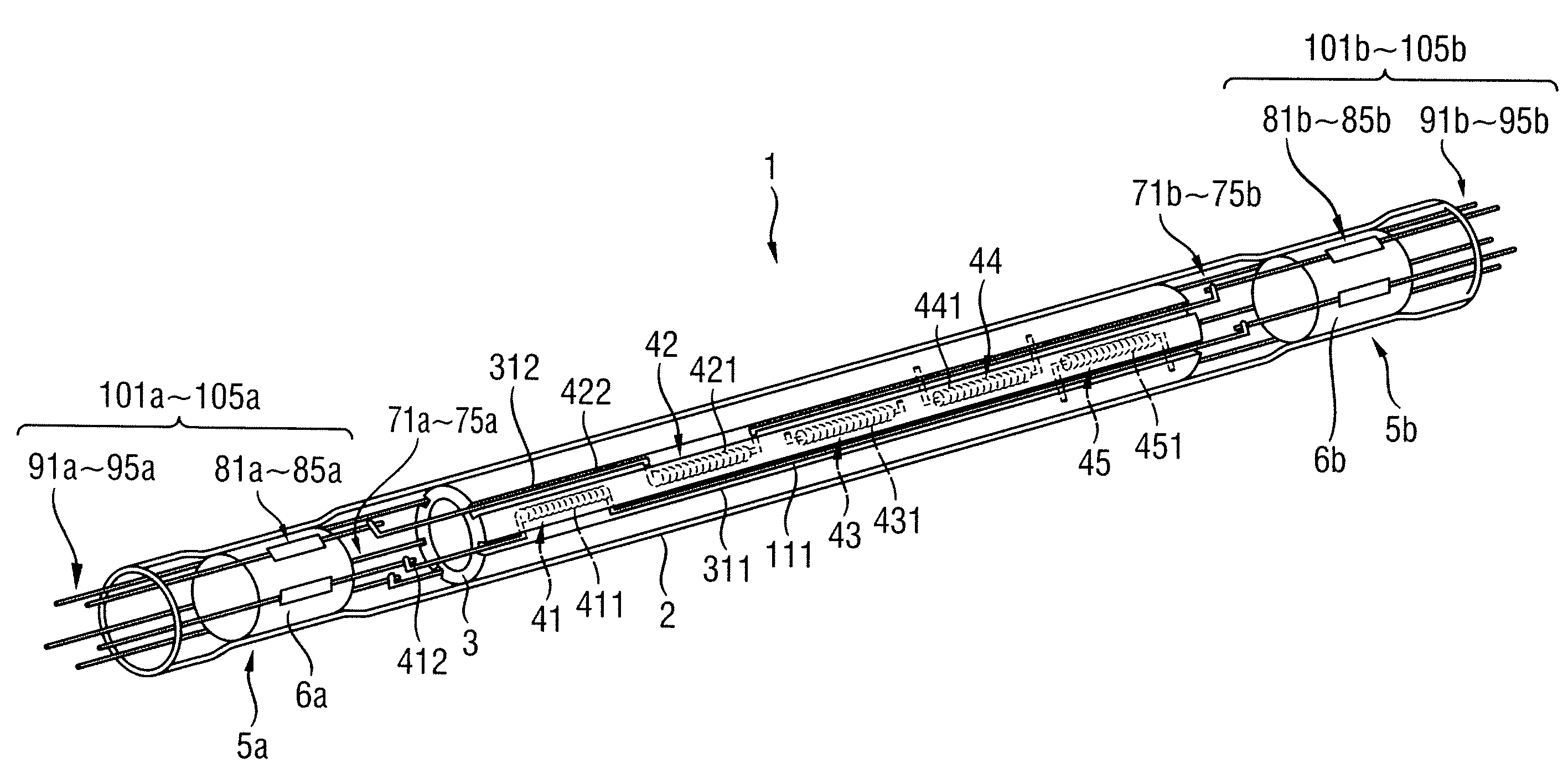
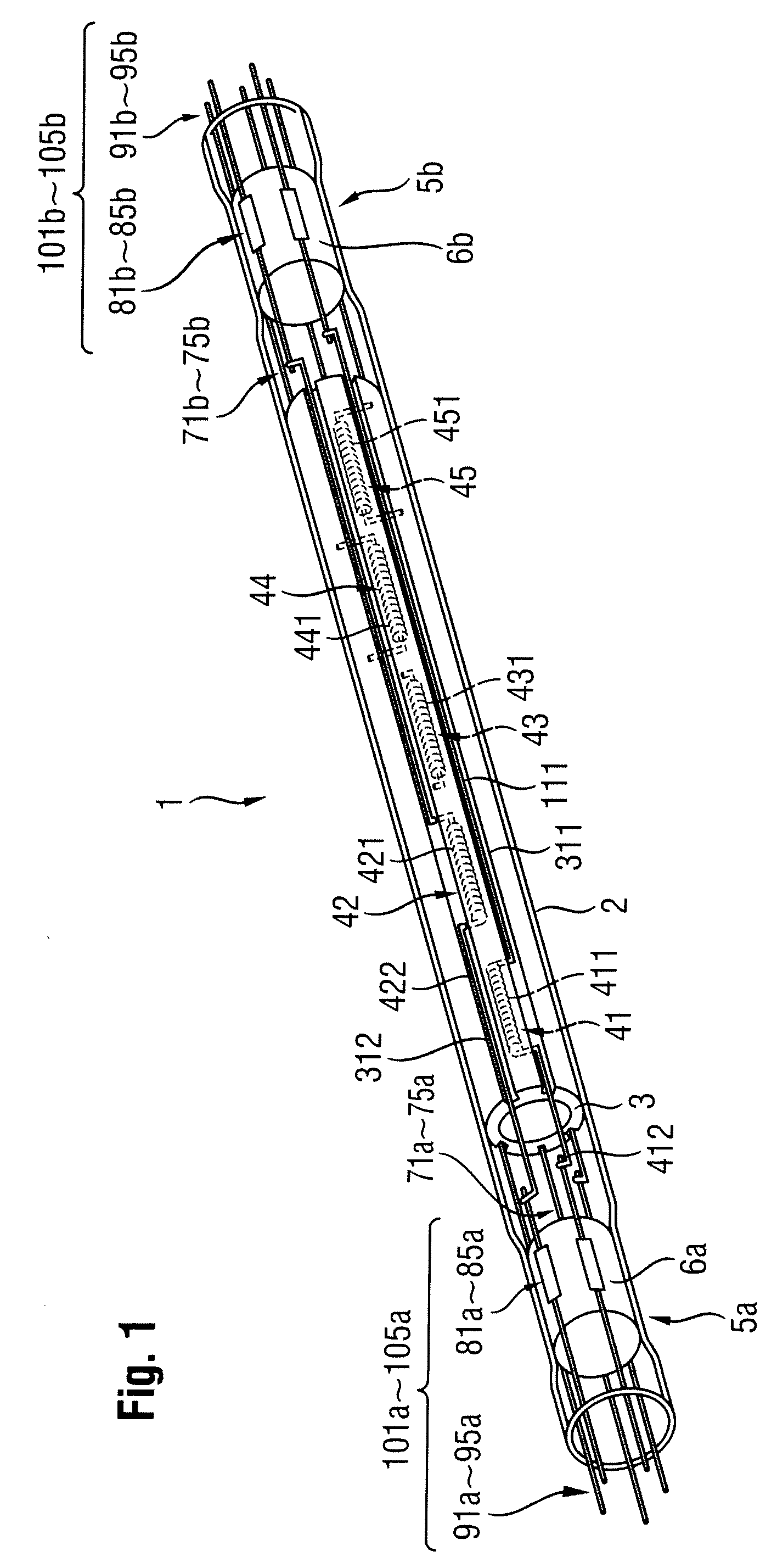
[0073]this invention is explained using FIGS. 1 through 6. FIG. 1 is a perspective view showing the constitution of the filament lamp 1 involved in the invention of this embodiment. As shown in FIG. 1, the filament lamp 1 has a linear or other tubular light emitting tube 3, made of quartz glass or another light-transparent material. Air-tight seal areas 5a, 5b are formed by fusing sealing insulators 6a, 6b on the light emitting tube 2 at both ends of the light emitting tube 2. A tubular insulating wall / inner tube 3, made of quartz glass or another light-transparent material and shorter in length in the direction of the tube axis of the light emitting tube 2, is located on the same axis as the light emitting tube 2 in proximity to the inner surface of the light emitting tube 2 within the light emitting tube 2, in which is sealed a halogen gas. For example, five filament assemblies 41 to 45 are located within this inner tube, and filaments 411 to 451 of the filament assemblies 41 to 4...

second embodiment

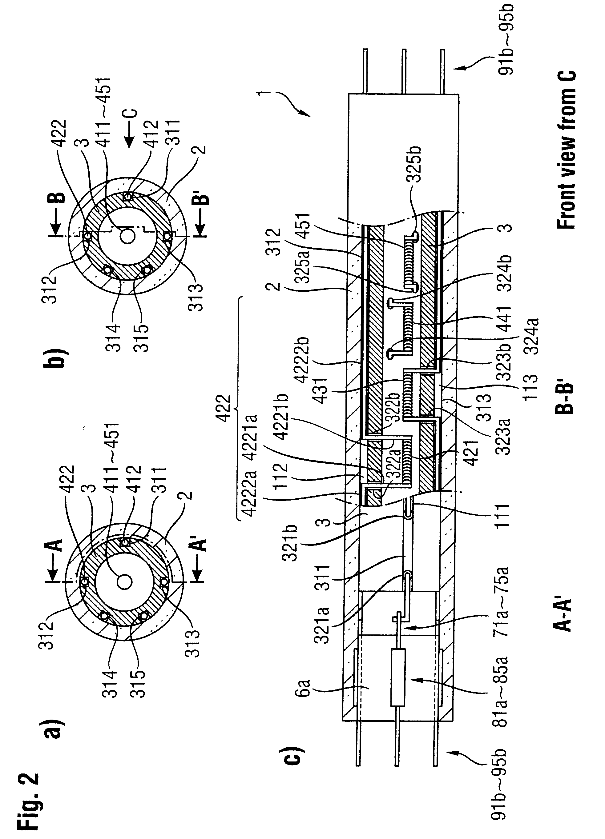
[0099]this invention is explained using FIGS. 7(a)-7(c), which are front cross-sectional views showing the filament lamp 1 of the invention of this embodiment, sectioned across and along the tube axis. FIGS. 7(a) &7(b) are cross sections of the filament lamp 1 cut in the radial direction. FIG. 7(c) has a cross section of the filament lamp 1 cut along the direction of the tube axis at line A-A′ in FIG. 7(a), a cross section of the filament lamp 1 cut along the direction of the tube axis at line B-B′ in FIG. 7(b), and a front view of the filament lamp 1 as seen from C in FIG. 7(b).

[0100]As shown in FIGS. 7(a)-7(c), the filament lamp 1 of the invention of this embodiment is not limited to the mode of lead accommodation spaces 111 to 115 formed by multiple slots 311 to 315 in the inner tube 3 and the inner surface of the light emitting tube 2, like the filament lamp 1 of the invention of the first embodiment. In this filament lamp 1, multiple slots 131 to 135 are formed in the inner sur...

third embodiment

[0104]this invention is explained using 8(a)-8(c), which are front cross-sectional views showing the filament lamp 1 of the invention of this embodiment, sectioned across and along the tube axis. FIGS. 8(a) &8(b) are cross sections of the filament lamp 1 cut in the radial direction. FIG. 8(c) has a cross section of the filament lamp 1 cut along the direction of the tube axis at line A-A′ in FIG. 8(a), a cross section of the filament lamp 1 cut along the direction of the tube axis at line B-B′ in FIG. 8(b), and a front view of the filament lamp 1 as seen from C in FIG. 8(b).

[0105]As shown in FIGS. 8(a)-8(c), in the filament lamp 1, multiple slots 131 to 135 are formed in the inner surface of the light emitting tube 13, extending along the tube axis and separated from each other in the circumferential direction. By placing an inner tube 15 close to the inner surface of this light emitting tube 13, one forms multiple lead accommodation spaces 111 to 115 demarcated by the slots 131 to 1...


PUM


Abstract

A filament lamp includes multiple filament assemblies having filaments connected to paired leads, arrayed in order within a light emitting tube and following a tube axis thereof. Each lead is electrically connected in a seal area. Each filament is powered independently. The light emitting tube includes insulating walls or inner tubes between the filaments and leads that have openings through which the leads pass, and located along the tube axis in proximity to the inner wall of the light emitting tube. Multiple lead accommodation spaces corresponding to the number of leads are provided in the light emitting tube by the insulating walls with each lead passing through an opening in the insulating wall and placed without short circuits in its lead accommodation space.

Description

FIELD OF INVENTION[0001]This invention concerns a filament lamp and light-irradiation-type heat treatment device, and particularly a filament lamp used for heat treatment of a workpiece and a light-irradiation-type heat treatment device equipped with such a filament lamp.DESCRIPTION OF RELATED ART[0002]Heat treatment is used in a variety of processes in the manufacture of semiconductors, including film growth, oxidation, nitriding, film stabilization, silicidation, crystallization, and ion injection activation. In particular, rapid thermal processing (hereafter referred to as “RTP”) of a semiconductor wafer or other workpiece to be treated by quickly raising and lowering its temperature enables improved throughput and quality, and so its use is desirable.[0003]Incandescent lamps, for example, are used as the light source in this sort of light-irradiation-type heat treatment device (hereafter referred to as “heat treatment device”).[0004]Incandescent lamps have filaments arranged ins...

Claims


Application Information

Patent Timeline
Patent Type & Authority Applications(United States)
IPC IPC(8): F26B3/28
CPCH01K1/16H01K1/24H01K1/38H01K7/00H01K9/08H01L21/67115H01S3/1618H05B3/0047H01L21/324
Inventor SUZUKI, SHINJINAKASHIMA, AKINOBUTANINO, KENJI
Owner USHIO DENKI KK
Why Eureka
Try Eureka