

Optical sensor element, optical sensor device and image display device using optical sensor element
a technology of optical sensors and optical sensors, applied in the direction of photovoltaic energy generation, semiconductor devices, electrical devices, etc., can solve the problems of increased cost due to mounting increased device operation, and increased cost of optical sensors and sensor drivers, etc., to suppress the increase in the number of steps, reduce the effect of noise characteristics and high sensitivity
- Summary
- Abstract
- Description
- Claims
- Application Information
AI Technical Summary
Benefits of technology
Problems solved by technology
Method used
Image

Examples
Embodiment Construction
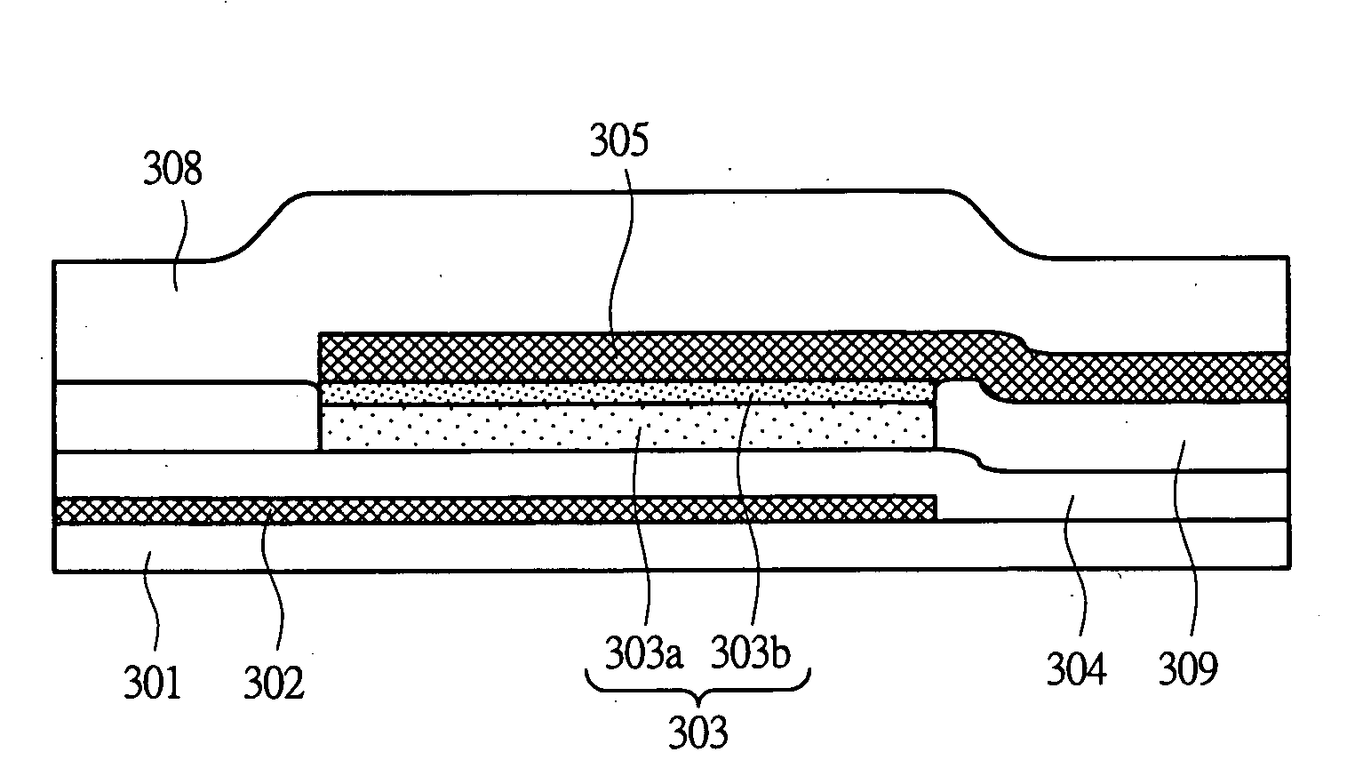
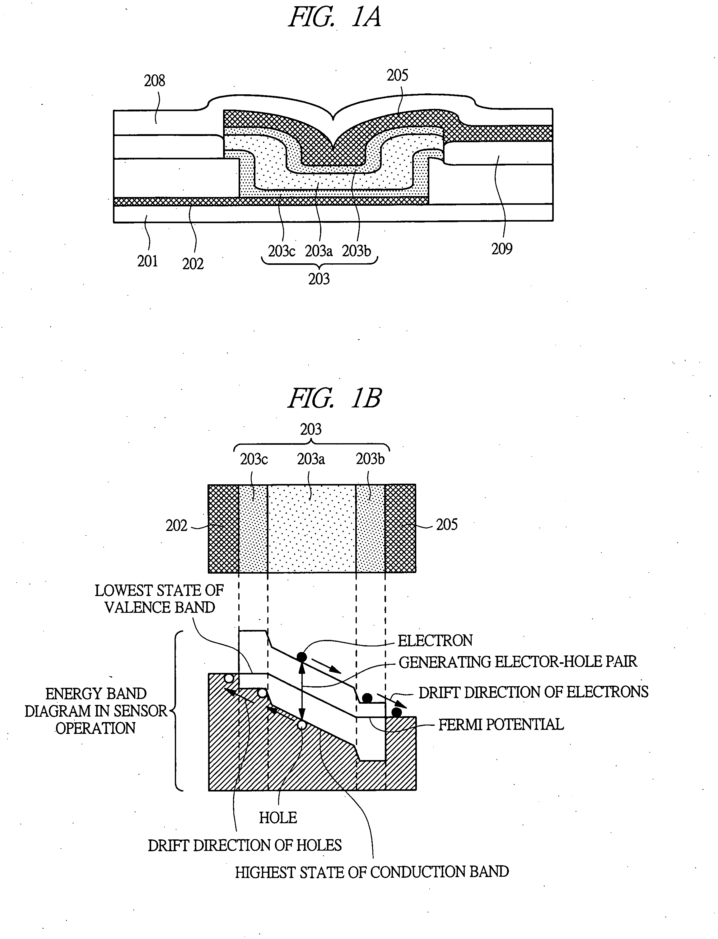
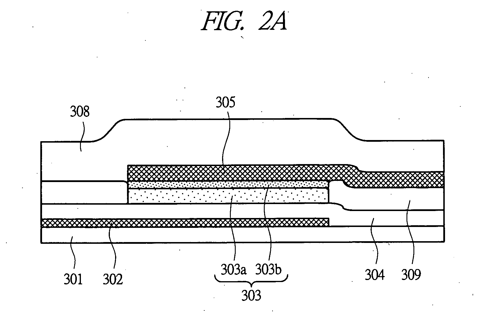
[0100]FIGS. 3A and 3B are conceptual diagrams of an optical sensor element according to the present invention. FIG. 3A is a cross-sectional view of the optical sensor element formed on an insulating substrate, and FIG. 3B is a top view thereof.
[0101]In FIG. 3A, a first electrode 2 composed of a polycrystalline silicon film 9 is formed on the insulating substrate 1, a photoelectric conversion layer 3 composed of an amorphous silicon film 10 is formed on the first electrode 2, and a second electrode (transparent electrode) 5 transparent to visible near-infrared light is further formed over the photoelectric conversion layer 3 through an insulating layer 4 (here, transparence to visible near-infrared light means that transmittance of energy of light in the range of 400 nm to 1000 nm is 75% or larger)
[0102]The first electrode 2 is connected to an interconnection (transparent electrode material) 6 via a contact hole 11. Although the example of FIGS. 3A and 3B show a case where the interc...
PUM
 Abstract
Description
Claims
Application Information