Strained Isolation Regions

Active Publication Date: 2008-12-11
TAIWAN SEMICON MFG CO LTD
View PDF15 Cites 9 Cited by
  • Summary
  • Abstract
  • Description
  • Claims
  • Application Information

AI Technical Summary

Benefits of technology

[0007]These and other problems are generally reduced, solved or circumvented, and technical advantages are generally achieved, by embodiments of the present

Problems solved by technology

This approach, however, can be difficult to process in addition to presenting junction leakage concerns as a result of the blanket semiconductor alloy layer.
The epitaxial growth of the semiconductor alloy layer, such as a silicon-germanium layer, can be costly and difficult to accurately control the level of germanium in the epitaxially grown semiconductor alloy layer.
In addition, the

Method used


Image

  • Strained Isolation Regions
  • Strained Isolation Regions
  • Strained Isolation Regions

Examples


Embodiment Construction

[0015]The making and using of the presently preferred embodiments are discussed in detail below. It should be appreciated, however, that the present invention provides many applicable inventive concepts that can be embodied in a wide variety of specific contexts. The specific embodiments discussed are merely illustrative of specific ways to make and use the invention, and do not limit the scope of the invention.

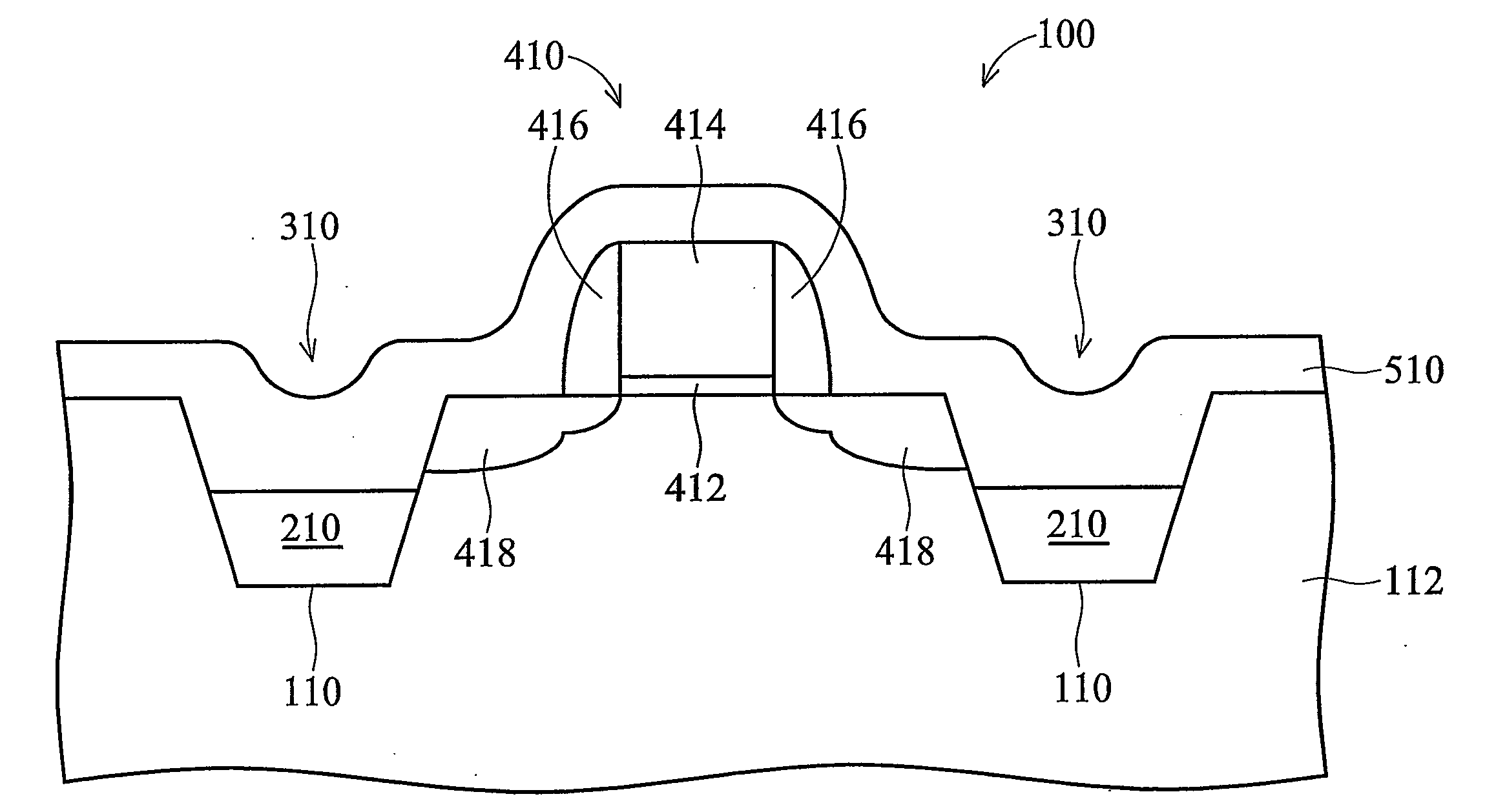
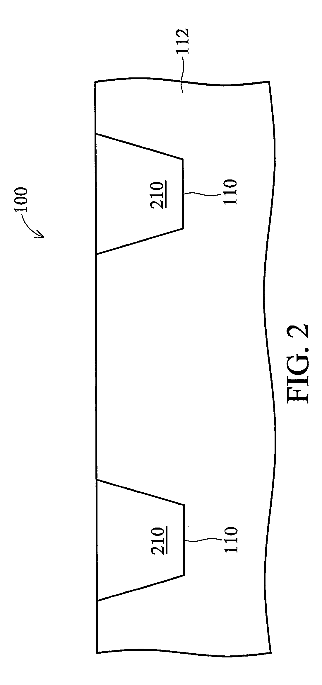
[0016]FIGS. 1-5 illustrate a method embodiment for fabricating a semiconductor device having a strained channel region in accordance with an embodiment of the present invention. Embodiments of the present invention illustrated herein may be used in a variety of circuits. Referring first to FIG. 1, a portion of a wafer 100 is shown comprising isolation trenches 110 formed in a substrate 112. The substrate 112 may comprise bulk silicon, doped or undoped, or an active layer of a semiconductor-on-insulator (SOI) substrate. Generally, an SOI comprises a layer of a semiconductor ma...


PUM


Abstract

An isolation trench having localized stressors is provided. In accordance with embodiments of the present invention, a trench is formed in a substrate and partially filled with a dielectric material. In an embodiment, the trench is filled with a dielectric layer and a planarization step is performed to planarize the surface with the surface of the substrate. The dielectric material is then recessed below the surface of the substrate. In the recessed portion of the trench, the dielectric material may remain along the sidewalls or the dielectric material may be removed along the sidewalls. A stress film, either tensile or compressive, may then be formed over the dielectric material within the recessed portion. The stress film may also extend over a transistor or other semiconductor structure.

Description

TECHNICAL FIELD[0001]The present invention relates generally to semiconductor devices, and more particularly, to metal-oxide-semiconductor field-effect transistors and methods of manufacture.BACKGROUND[0002]Size reduction of metal-oxide-semiconductor field-effect transistors (MOSFETs), including reduction of the gate length and gate oxide thickness, has enabled the continued improvement in speed, performance, density, and cost per unit function of integrated circuits over the past few decades. To further enhance transistor performance, MOSFET devices have been fabricated using strained channel regions located in portions of a semiconductor substrate. Strained channel regions allow enhanced carrier mobility to be realized, thereby resulting in increased performance when used for n-channel (NMOSFET) or for p-channel (PMOSFET) devices. Generally, it is desirable to induce a tensile strain in the n-channel of an NMOSFET transistor in the source-to-drain direction to increase electron mo...

Claims


Application Information

Patent Timeline
IPC IPC(8): H01L29/78
CPCH01L21/76224H01L29/7833H01L29/1054H01L29/7846H01L29/7843
Inventor LIANG, MONG-SONGLEE, TZE-LIANGHUANG, KUO-TAICHEN, CHAO-CHENGLIEN, HAO-MINGPENG, CHIH-TANG
Owner TAIWAN SEMICON MFG CO LTD
Why Eureka
Try Eureka