Reverse masking profile improvements in high aspect ratio etch
a technology of reverse masking and aspect ratio etching, applied in the direction of basic electric elements, electrical equipment, semiconductor devices, etc., can solve the problems of lateral electrical field, negative charging of the top of the feature, and increasing the problem of twisting
- Summary
- Abstract
- Description
- Claims
- Application Information
AI Technical Summary
Problems solved by technology
Method used
Image

Examples
Embodiment Construction
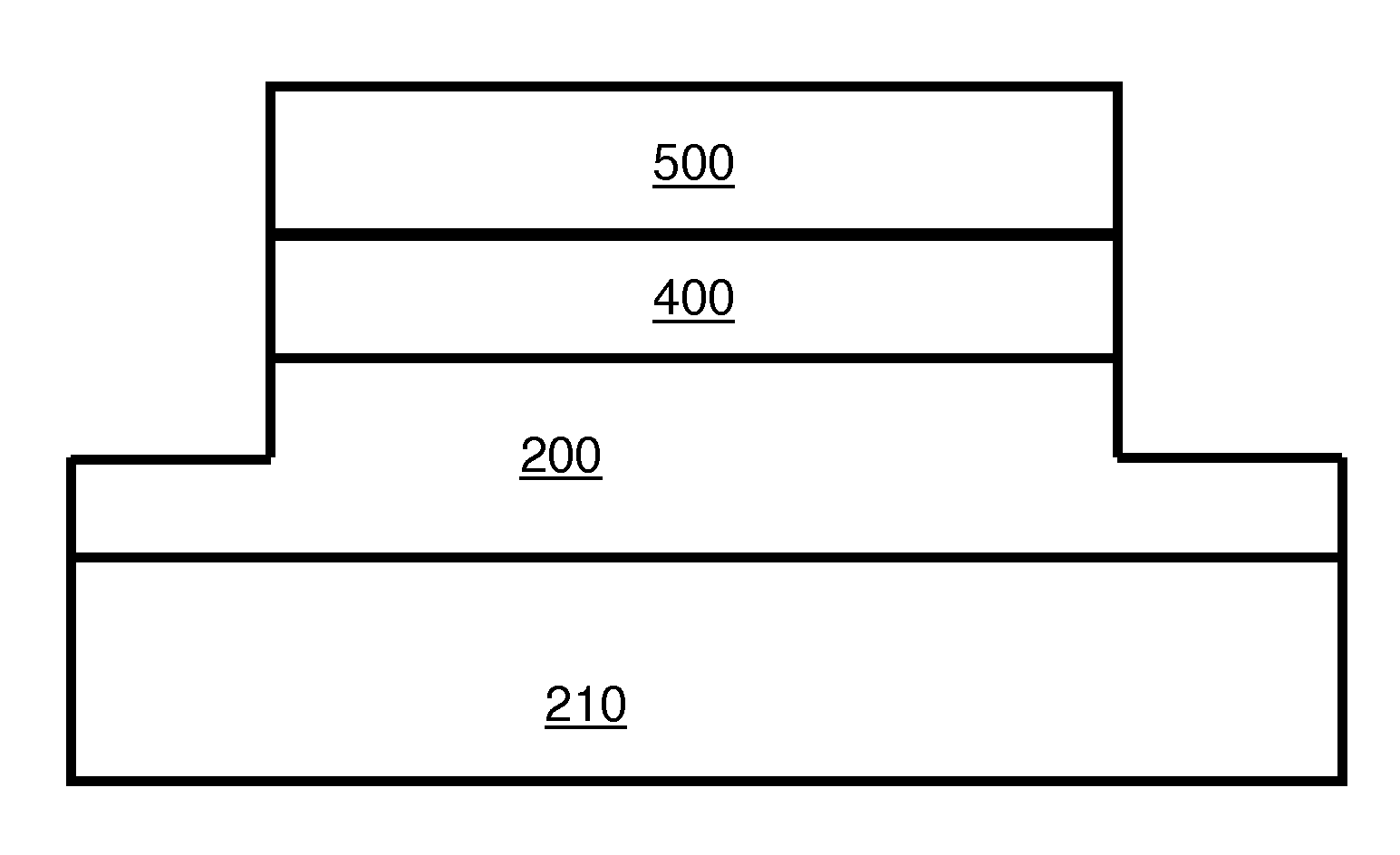
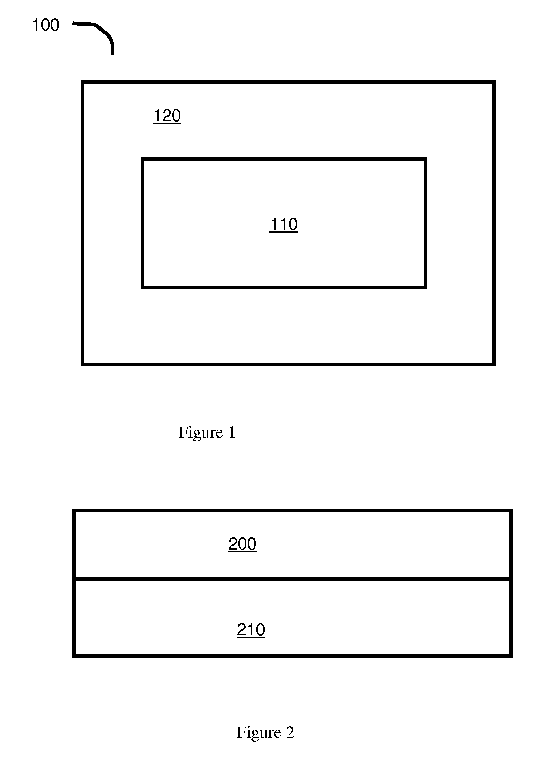
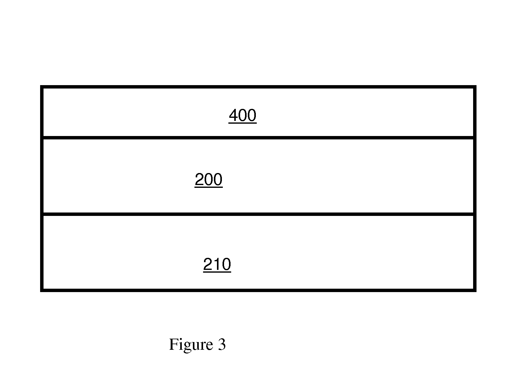
[0011]In the following detailed description of the embodiments, reference is made to the accompanying drawings that form a part hereof, and in which are shown by way of illustration, and not by way of limitation, specific embodiments in which the invention may be practiced. It is to be understood that other embodiments may be utilized and that logical, mechanical and electrical changes may be made without departing from the spirit and scope of the present invention.
[0012]The term ‘substrate’ is to be understood as a semiconductor-based material including silicon, silicon-on-insulator (SOI) or silicon-on-sapphire (SOS) technology, doped and undoped semiconductors, epitaxial layers of silicon supported by a base semiconductor foundation, and other semiconductor structures. Further, in the discussion and claims herein, the term ‘on’ used with respect to two layers, one ‘on’ the other, means at least some contact between the layers, while ‘over’ means the layers are in close proximity, ...
PUM
| Property | Measurement | Unit |
|---|---|---|
| aspect ratio | aaaaa | aaaaa |
| aspect ratio | aaaaa | aaaaa |
| aspect ratio | aaaaa | aaaaa |
Abstract
Description
Claims
Application Information
 - Generate Ideas
- Intellectual Property
- Life Sciences
- Materials
- Tech Scout
- Unparalleled Data Quality
- Higher Quality Content
- 60% Fewer Hallucinations
Browse by: Latest US Patents, China's latest patents, Technical Efficacy Thesaurus, Application Domain, Technology Topic, Popular Technical Reports.
© 2025 PatSnap. All rights reserved.Legal|Privacy policy|Modern Slavery Act Transparency Statement|Sitemap|About US| Contact US: help@patsnap.com