Capacitor-Less Memory

a technology of capacitors and memory elements, applied in the direction of semiconductor devices, electrical apparatus, transistors, etc., can solve the problems of increasing the driving voltage of memory elements, reducing the generation efficiency of electrons and holes by hot carriers, etc., and achieves the reduction of the effect of reducing the number of common lines and simple structur

Inactive Publication Date: 2008-12-18
SEMICON ENERGY LAB CO LTD
View PDF8 Cites 10 Cited by
  • Summary
  • Abstract
  • Description
  • Claims
  • Application Information

AI Technical Summary

Benefits of technology

[0021]According to another aspect of the present invention, a capacitor-less memory is provided in which a plurality of transistors having the above structure is included, and a plurality of word lines each connected to respective gate electrodes of the transistors, a plurality of common lines each connected to respective source regions of the transistors, and a plurality of bit lines each connected to respective drain regions of the transistors are included. The common lines and the bit lines extend almost in parallel and are almost perpendicular to the word lines. The transistors which are adjacent to each other between one of a plurality of common lines in a direction a

Problems solved by technology

Note that, similarly to the source region, the drain region can also be formed of a semiconductor having a larger band gap than the semiconductor of the active layer region; however, when the band ga

Method used


Image

  • Capacitor-Less Memory
  • Capacitor-Less Memory
  • Capacitor-Less Memory

Examples


Embodiment Construction

Embodiment Mode

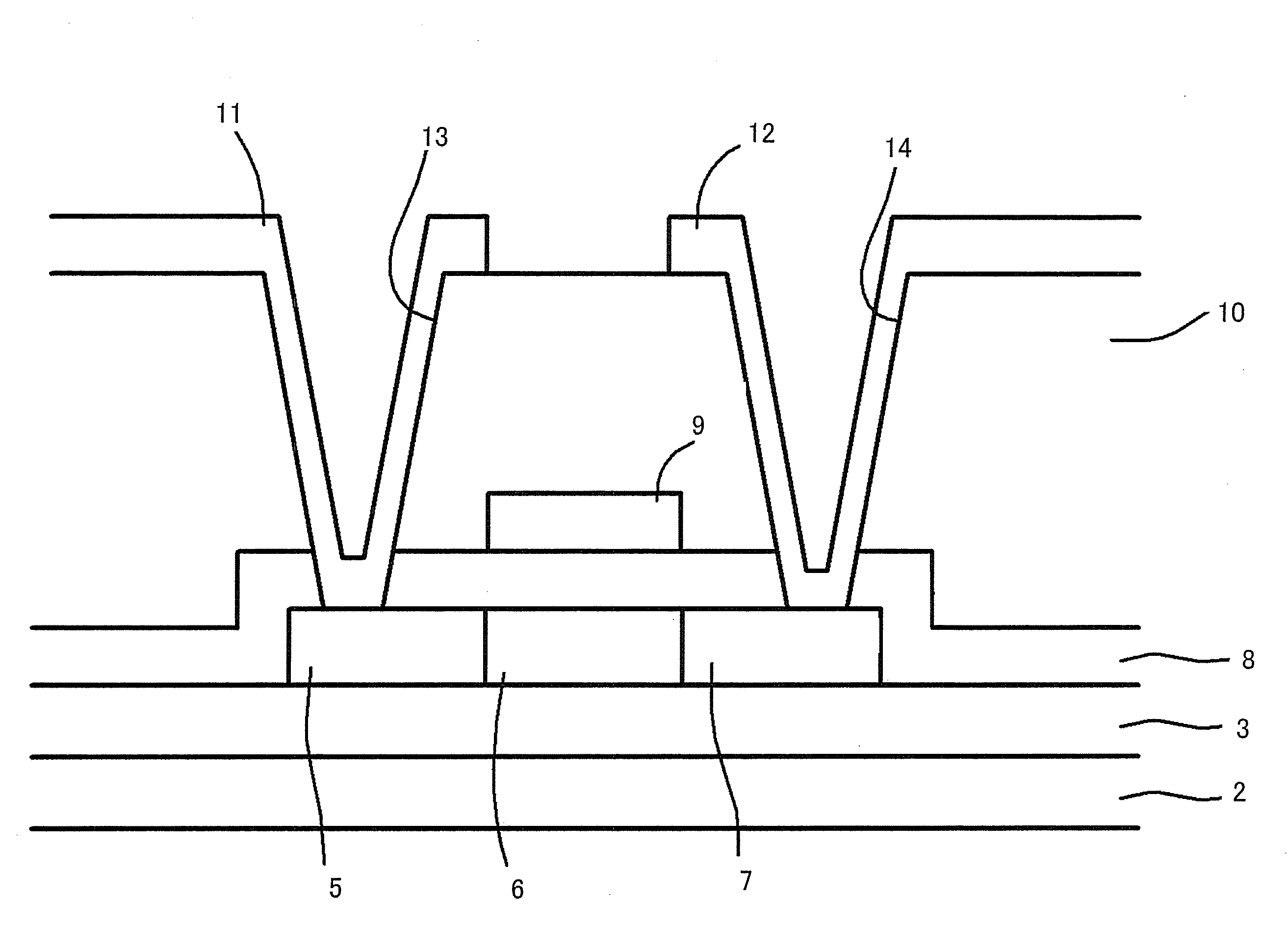
[0056]FIG. 3 is a cross-sectional view which shows a preferred embodiment of a transistor that can be used as a memory cell of a capacitor-less memory based on the present invention. In this transistor, a silicon oxynitride film is formed as a base insulating film 3 over a substrate 2 which is formed of a glass substrate or the like, and an island-shaped semiconductor film that includes a source region 5, an active layer region 6, and a drain region 7 is formed over the base insulating film 3. A gate electrode 9 formed of tantalum nitride is formed over the active layer region 6, so that a gate insulating film 8 formed of yttrium oxide is interposed therebetween. An interlayer insulating film 10 that has a planarized surface formed of silicon oxynitride is provided over the gate electrode 9, and conductive films 11 and 12 that are formed by stacking a titanium film, an aluminum film, and a titanium film are formed over the interlayer insulating film 10. Contact openin...


PUM


Abstract

It is an object of the present invention to provide a capacitor-less memory which can prevent a change of a threshold voltage due to flowing out of carriers and improve the memory retention property without a complicated structure. In the capacitor-less memory which uses a transistor, the transistor includes a source region, a drain region, an active layer region which is provided between the source region and the drain region, and a gate electrode which is adjacent to the active layer region with an insulating film interposed therebetween. The source region is formed of a semiconductor having a larger band gap than a band gap of a semiconductor of the active layer region and a band gap of a semiconductor of the drain region, and a heterojunction is formed at the interface between the source region and the active layer region.

Description

BACKGROUND OF THE INVENTION[0001]1. Field of the Invention[0002]The present invention relates to a capacitor-less memory. In particular, the present invention relates to a capacitor-less memory including a transistor that has both functions of selecting a memory cell and retaining information.[0003]2. Description of the Related Art[0004]For higher integration of a DRAM, so-called capacitor-less DRAM without a capacitor (storage capacitor) to hold charge has attracted attention (see e.g., Reference 1: Japanese Published Patent Application No. 2002-246571, Reference 2: Japanese Published Patent Application No. H8-213624, and Reference 3: Japanese Published Patent Application No. H10-92952). Unlike a conventional DRAM that stores charge in a storage capacitor, a capacitor-less DRAM stores charge in a switching transistor. In the capacitor-less DRAM, since the switching transistor has both functions of selecting a memory cell and retaining information, the storage capacitor is not neede...

Claims


Application Information

Patent Timeline
IPC IPC(8): H01L29/04H01L29/78
CPCH01L27/108H01L27/10802H01L29/78654H01L29/78618H01L29/7841H10B12/20H10B12/00H10B99/00
Inventor HONDA, TATSUYA
Owner SEMICON ENERGY LAB CO LTD
Why Eureka
Try Eureka