Display device and manufacturing method thereof

a technology a manufacturing method, which is applied in the direction of semiconductor devices, instruments, electrical appliances, etc., can solve the problems of increasing the cost, reducing the yield, and requiring a more complicated process, so as to prevent the mobility of a thin film transistor from decreasing, the deposition rate of a microcrystalline semiconductor film can be increased, and the mass productivity of a display device can be increased.

Inactive Publication Date: 2008-12-18
SEMICON ENERGY LAB CO LTD
View PDF30 Cites 174 Cited by
  • Summary
  • Abstract
  • Description
  • Claims
  • Application Information

AI Technical Summary

Benefits of technology

[0021]In the present invention, an antioxidant film is formed on a surface of a microcrystalline semiconductor film and thus oxidation of a surface of a microcrystal grain can be reduced, thereby preventing the mobility of a thin film transistor from decreasing.
[0022]With use of a microwave plasma CVD apparatus with a frequency of 1 GHz or more, a deposition rate of a microcrystalline semiconductor film can be increased, and mass productivity of a display device including a thin film transistor including the microcrystalline semiconductor film can be improved.
[0023]In addition, a crystallization process of a semiconductor film after formation of the semiconductor film can be omitted, so that a system-on-panel of the display device can be achieved without complicating a manufacturing process of the thin film transistor.

Problems solved by technology

However, the thin film transistor using a polycrystalline semiconductor film for a channel formation region requires a more complicated process than the thin film transistor using an amorphous semiconductor film for a channel formation region because of crystallization of the semiconductor film.
Thus, there are problems such as a reduction in yield and an increase in cost.
Further, there is a problem in that a surface of a crystal grain of a semiconductor is easily oxidized.

Method used


Image

  • Display device and manufacturing method thereof
  • Display device and manufacturing method thereof
  • Display device and manufacturing method thereof

Examples


embodiment modes

[0047]Hereinafter, embodiment modes of the present invention are described with reference to the drawings. It is easily understood by those skilled in the art that the modes and details disclosed herein can be modified in various ways without departing from the spirit and scope of the present invention. Therefore, the present invention should not be interpreted as being limited to the description of the embodiment modes to be given below.

embodiment mode 1

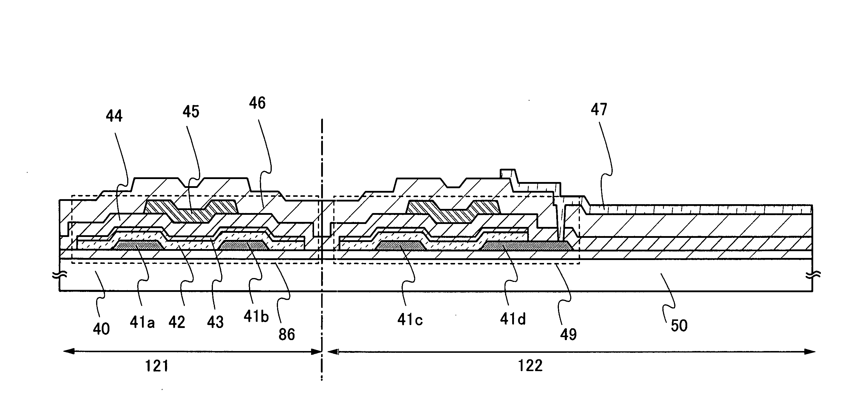
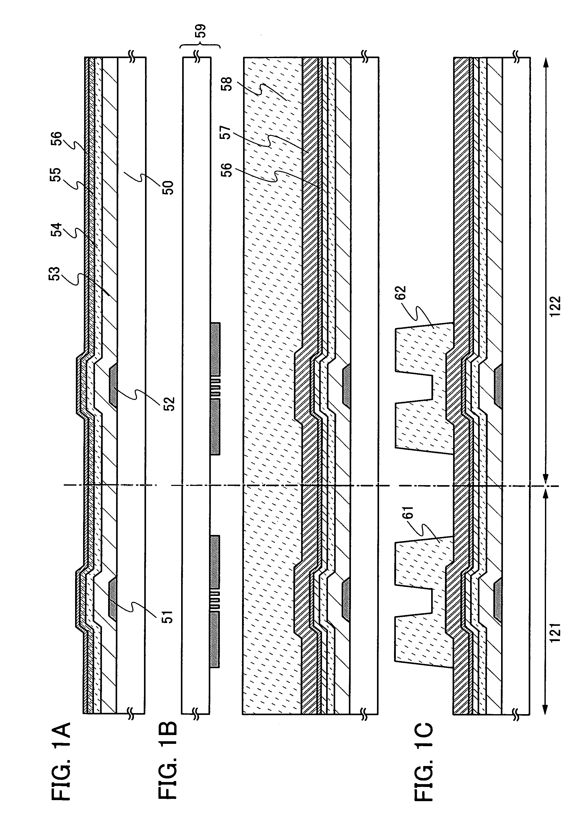
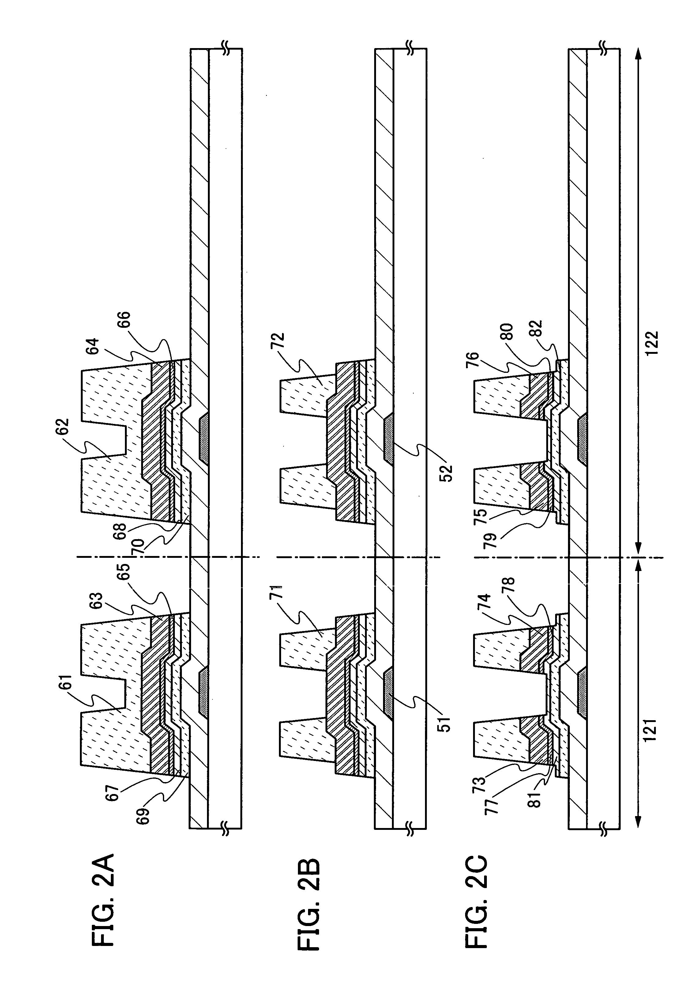
[0048]A method for manufacturing a display device of the present invention is described. First, the description is made using a liquid crystal device, which is one mode of the display device. FIGS. 1A to 3B are cross-sectional views illustrating a thin film transistor used for a driver circuit and a thin film transistor used for a pixel portion. With regard to a thin film transistor including a microcrystalline semiconductor film, an n-channel thin film transistor has higher mobility than a p-channel thin film transistor; thus, an n-channel thin film transistor is more suitable for a driver circuit. However, in the present invention, either an n-channel or p-channel thin film transistor can be used. With any polarity of a thin film transistor, it is preferable that all the thin film transistors formed over one substrate have the same polarity so that the number of manufacturing steps is reduced.

[0049]As illustrated in FIG. 1A, gate electrodes 51 and 52 are formed over a substrate 50...

embodiment mode 2

[0192]This embodiment mode describes a structure of a display panel, which is one mode of the display device of the present invention.

[0193]FIG. 15A illustrates a mode of a display panel in which a pixel portion 6012 formed over a substrate 6011 is connected to a signal line driver circuit 6013 that is formed separately. The pixel portion 6012 and a scanning line driver circuit 6014 are each formed using a thin film transistor including a microcrystalline semiconductor film. By forming the signal line driver circuit with a thin film transistor by which higher mobility can be obtained compared to the thin film transistor including the microcrystalline semiconductor film, operation of the signal line driver circuit, which demands a higher driving frequency than that of the scanning line driver circuit, can be stabilized. The signal line driver circuit 6013 may be formed using a thin film transistor including a single-crystalline semiconductor, a thin film transistor including a polycr...


PUM


Abstract

It is an object to provide a manufacturing method by which display devices can be manufactured in quantity without degrading the characteristics of thin film transistors. In a display device including a thin film transistor in which a microcrystalline semiconductor film, a gate insulating film in contact with the microcrystalline semiconductor film, and a gate electrode overlap with each other, an antioxidant film is formed on a surface of the microcrystalline semiconductor film. The antioxidant film on the surface of the microcrystalline semiconductor film can prevent a surface of a microcrystal grain from being oxidized, thereby preventing the mobility of the thin film transistor from decreasing.

Description

BACKGROUND OF THE INVENTION[0001]1. Field of the Invention[0002]The present invention relates to a display device in which a thin film transistor is used at least in a pixel portion.[0003]2. Description of the Related Art[0004]In recent years, technology that is used to form thin film transistors using semiconductor thin films (with thicknesses of from several tens of nanometers to several hundreds of nanometers, approximately) formed over substrates having an insulating surface, for channel formation regions, has been attracting attention. Thin film transistors are applied to a wide range of electronic devices such as ICs or electro-optical devices, and prompt development of thin film transistors that are to be used as switching elements in image display devices, in particular, is being pushed.[0005]As a switching element in an image display device, a thin film transistor in which an amorphous semiconductor film is used for a channel formation region, a thin film transistor in whic...

Claims


Application Information

Patent Timeline
Patent Type & Authority Applications(United States)
IPC IPC(8): H01L29/04H01L21/314
CPCH01L21/3145H01L27/1214H01L27/1288H01L29/78696H01L29/78606H01L21/0214H01L21/02274
Inventor YAMAZAKI, SHUNPEIICHIJO, MITSUHIROTANAKA, TETSUHIROOHTSUKI, TAKASHIYASUMOTO, SEIJIOKAZAKI, KENICHI
Owner SEMICON ENERGY LAB CO LTD
Why Eureka
Try Eureka