Display device

a display device and pixel structure technology, applied in the direction of discharge tube/lamp details, discharge tube luminescnet screens, organic semiconductor devices, etc., can solve the problems of difficult stable hole injection and rough surface, and achieve the effect of lowering wiring resistance and high reflectivity

Active Publication Date: 2008-12-18
SAMSUNG DISPLAY CO LTD
View PDF5 Cites 25 Cited by
  • Summary
  • Abstract
  • Description
  • Claims
  • Application Information

AI Technical Summary

Benefits of technology

[0030]In the present invention, a display device which realizes high reflectivity and a lowered wiring resistance can be provided.

Problems solved by technology

In cases where the aluminum (hereafter indicated as “Al”) of the pixel electrodes of a TE-type AM-OLED is stripped away as in Japanese Laid-Open Patent Publication No. 2007-103098, the surface tends to become rough as a result of hillocks and the like that are generated when banks on top of the pixel electrodes are etched, and stable hole injection becomes difficult.

Method used


Image

  • Display device
  • Display device
  • Display device

Examples


example 1

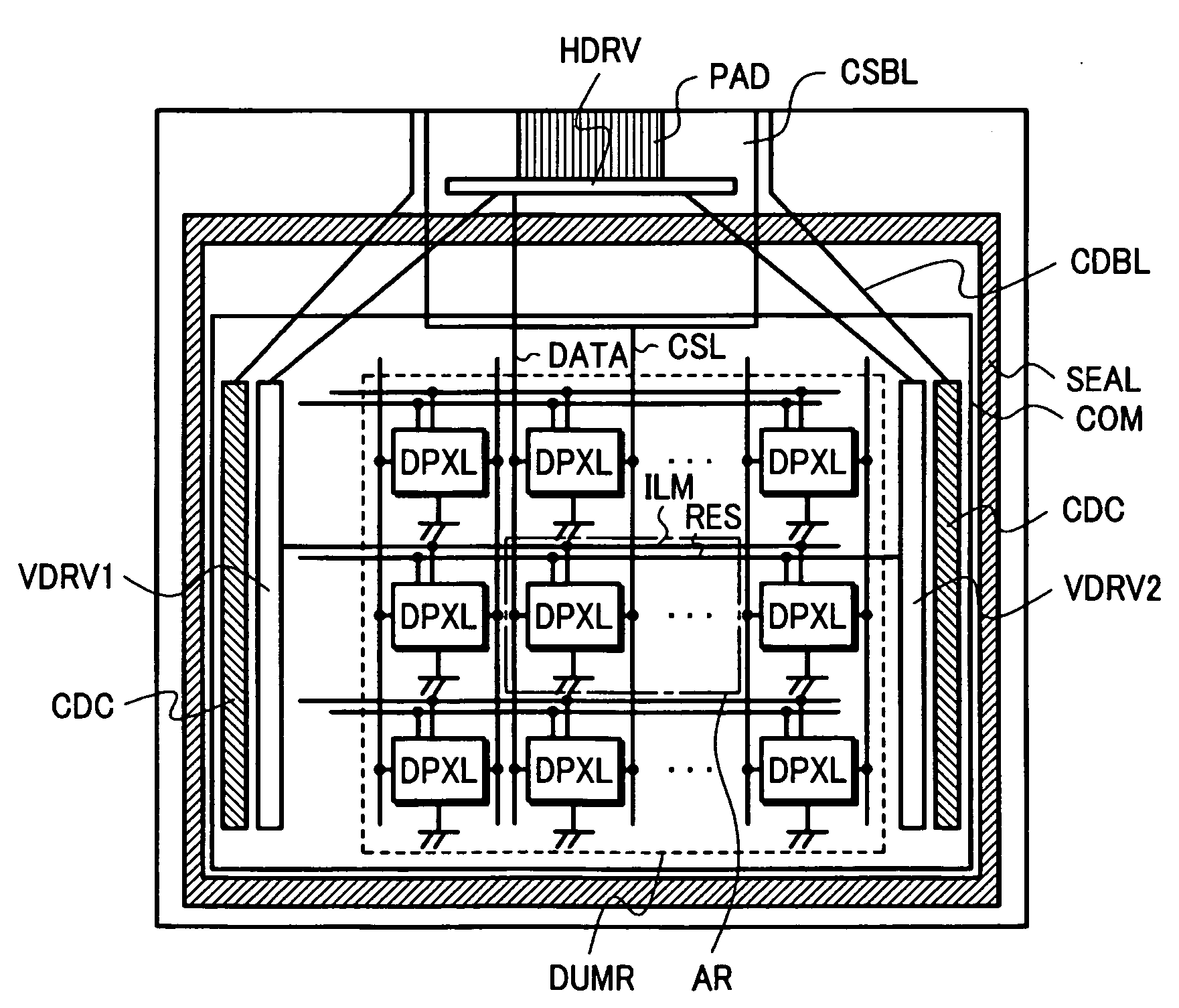
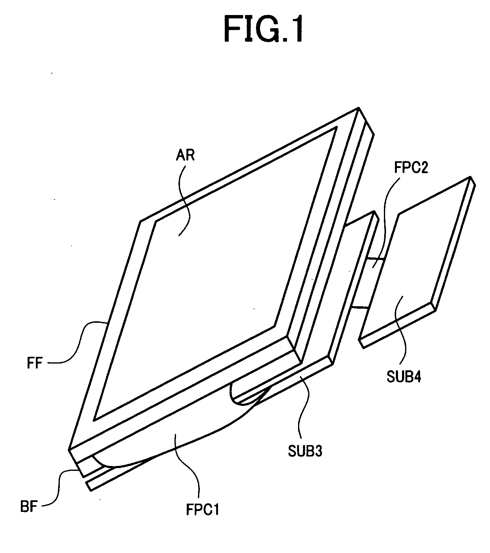
[0056]FIG. 1 is a view showing the external appearance of an organic EL display device. This organic EL display device has a structure comprising a front-surface frame FF having an opening that exposes the display area AR of an organic EL display panel (hereafter also referred to simply as a “panel”), a back-surface frame BF which covers the entire back surface of the organic EL display panel and which is fastened to the front-surface frame FF, a third substrate SUB3 which is further disposed on the back surface of the back-surface frame BF, a first flexible circuit board FPC1 which is attached between the terminals PAD of the third substrate SUB3 and the organic EL display panel, a fourth substrate SUB4, and a second flexible circuit board FPC2 which connects the third substrate SUB3 and fourth substrate SUB4.

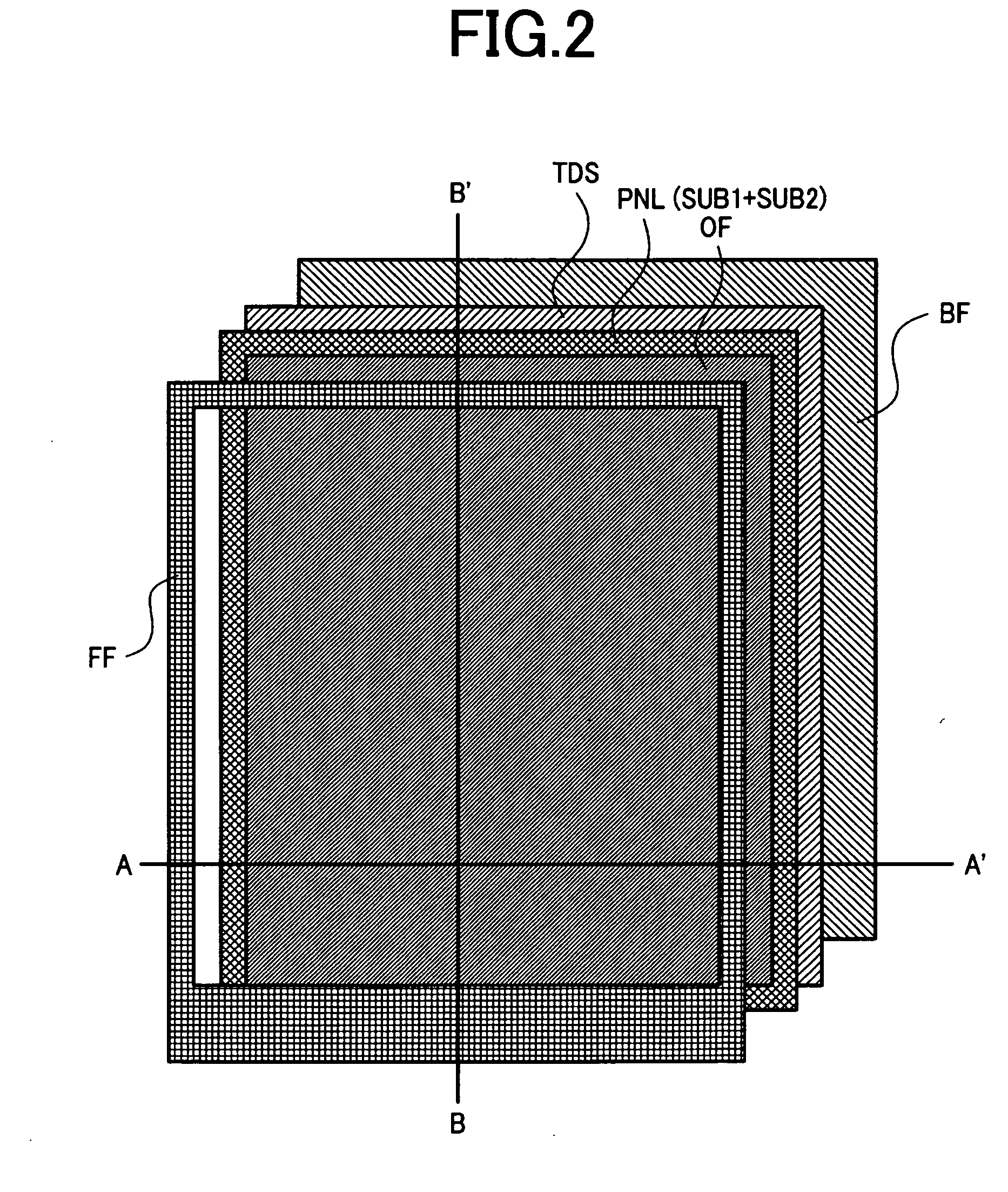
[0057]The cross-sectional structure of the organic EL display panel sandwiched between the front-surface frame FF and back-surface frame BF will be described with reference to...


PUM


Abstract

There is provided a display device comprising a plurality of active elements on a substrate, a first insulating film for covering the active elements, electroconductive films were separated for each pixel on the first insulating film, a light-emitting layer disposed in an upper layer of the electroconductive films, and a common electrode disposed in an upper layer of the light-emitting layer, wherein a structure is used in which the electroconductive films have a layered film of a first electroconductive film, second electroconductive film, and third electroconductive film; the first electroconductive film is composed of ITO or chromium; the second electroconductive film is composed of aluminum with alumina on a surface; the second electroconductive film covers outside edges of the first electroconductive film; the third electroconductive film is composed of ITO; and the first electroconductive film and third electroconductive film are caused to contact each other.

Description

CROSS-REFERENCE TO RELATED APPLICATION[0001]The present application claims priority from Japanese application JP2007-146454 filed on Jun. 1, 2007, the content of which is hereby incorporated by reference into this application.BACKGROUND OF THE INVENTION[0002]1. Field of the Invention[0003]The present invention relates to the pixel structure of a display device.[0004]2. Description of the Related Art[0005]Organic EL display devices (organic electroluminescent display devices) constitute one-type of an active matrix display device.[0006]If such organic EL display devices are classified according to the relationship between the orientation of the display surface and the surface on which organic EL elements are formed, these display devices can be roughly divided into (1) bottom emission-type display devices in which the back surface side of the surface on which the organic EL elements are formed is used as the front surface, and (2) top emission-type display devices in which the surfac...

Claims


Application Information

Patent Timeline
Patent Type & Authority Applications(United States)
IPC IPC(8): H01J1/62
CPCH01L27/3244H01L51/5218H01L51/5228H01L51/5271H01L2251/5315H05B33/10H05B33/26H01L27/3248H10K59/12H10K50/818H10K50/824H10K50/856H10K2102/3026H10K59/123
Inventor HASEGAWA, ATSUSHITOKUDA, NAOKI
Owner SAMSUNG DISPLAY CO LTD
Why Eureka
Try Eureka