Method to form low-defect polycrystalline semiconductor material for use in a transistor

a technology of polycrystalline semiconductors and transistors, applied in the direction of semiconductor devices, basic electric elements, electrical equipment, etc., can solve the problems of affecting the performance of thin film transistors, destroying or ruining the devices,

Active Publication Date: 2008-12-18
SANDISK TECH LLC
View PDF27 Cites 19 Cited by
  • Summary
  • Abstract
  • Description
  • Claims
  • Application Information

AI Technical Summary

Benefits of technology

[0006]A first aspect of the invention provides for method for forming a current switching region in a thin film transistor, the method comprising: forming a feature comprising amorphous silicon, amorphous germanium, or amorphous silicon-germanium, said feature having a width in at least one dimension of about 0.25 microns or less; forming a titanium film on and in contact with said feature; annealing said feature and said titanium film to form titanium silicide, titanium germanide, or titanium silicide-germanide and to crystallize said amorphous silicon, said amorphous germanium, or said amorphous silicon-germanium of said feature to form polycrystalline silicon, polycrystalline germanium, or polycrystalline silicon-germanium; and forming the thin film transistor, wherein said polycrystalline silicon feature, said polycrystalline germanium feature, or said polycrystalline silicon-germanium feature comprises the current switching region of the thin film transistor.
[0007]Another aspect of the invention provides for a method for forming a monolithic three dimensional array, the method comprising: a) monolithically forming a first dev

Problems solved by technology

In general the performance of thin film transistors is impeded by grain boundaries and crystal defects in the semiconductor material in which the current-switching region of the

Method used


Image

  • Method to form low-defect polycrystalline semiconductor material for use in a transistor
  • Method to form low-defect polycrystalline semiconductor material for use in a transistor
  • Method to form low-defect polycrystalline semiconductor material for use in a transistor

Examples


first embodiment

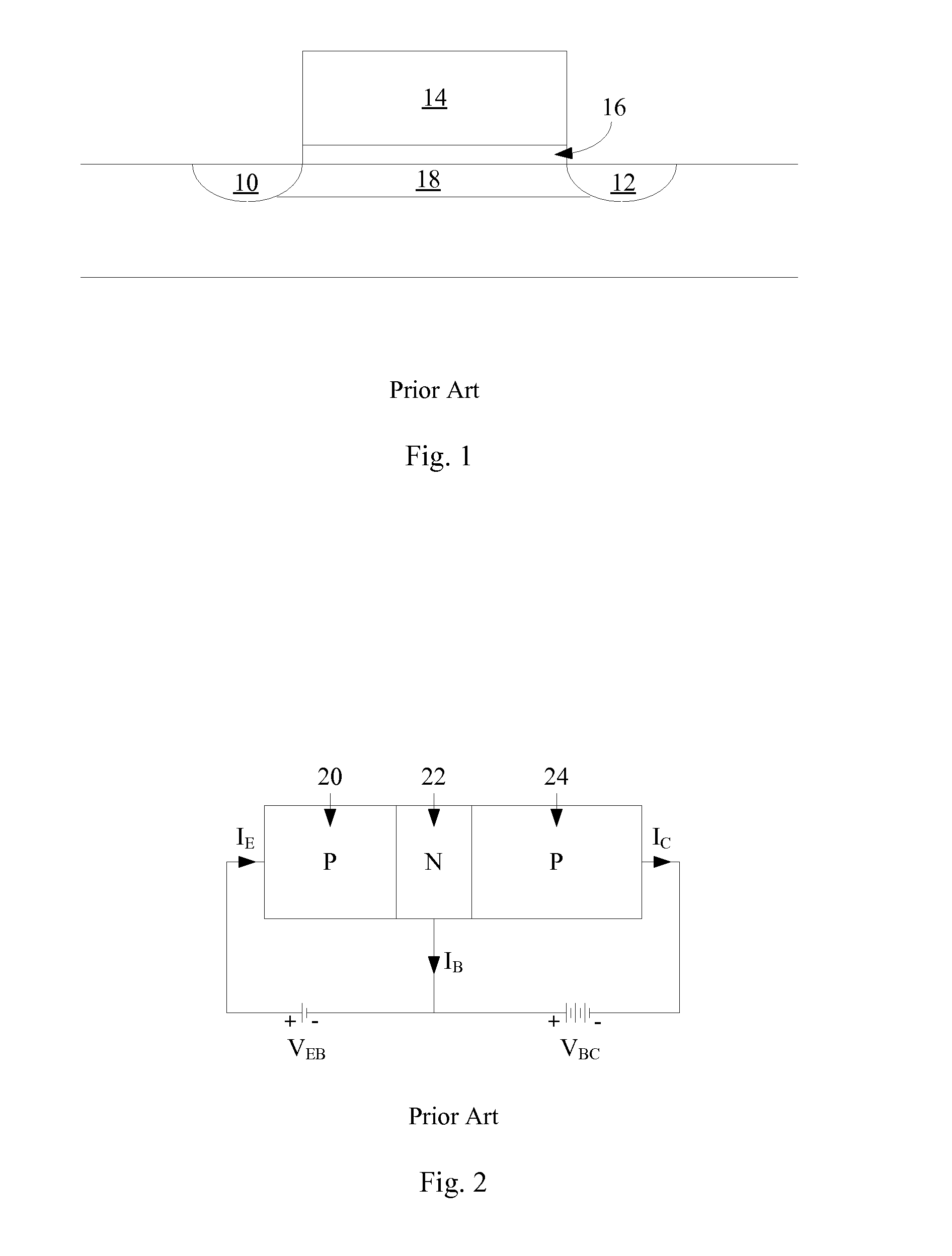
Field-Effect Transistor

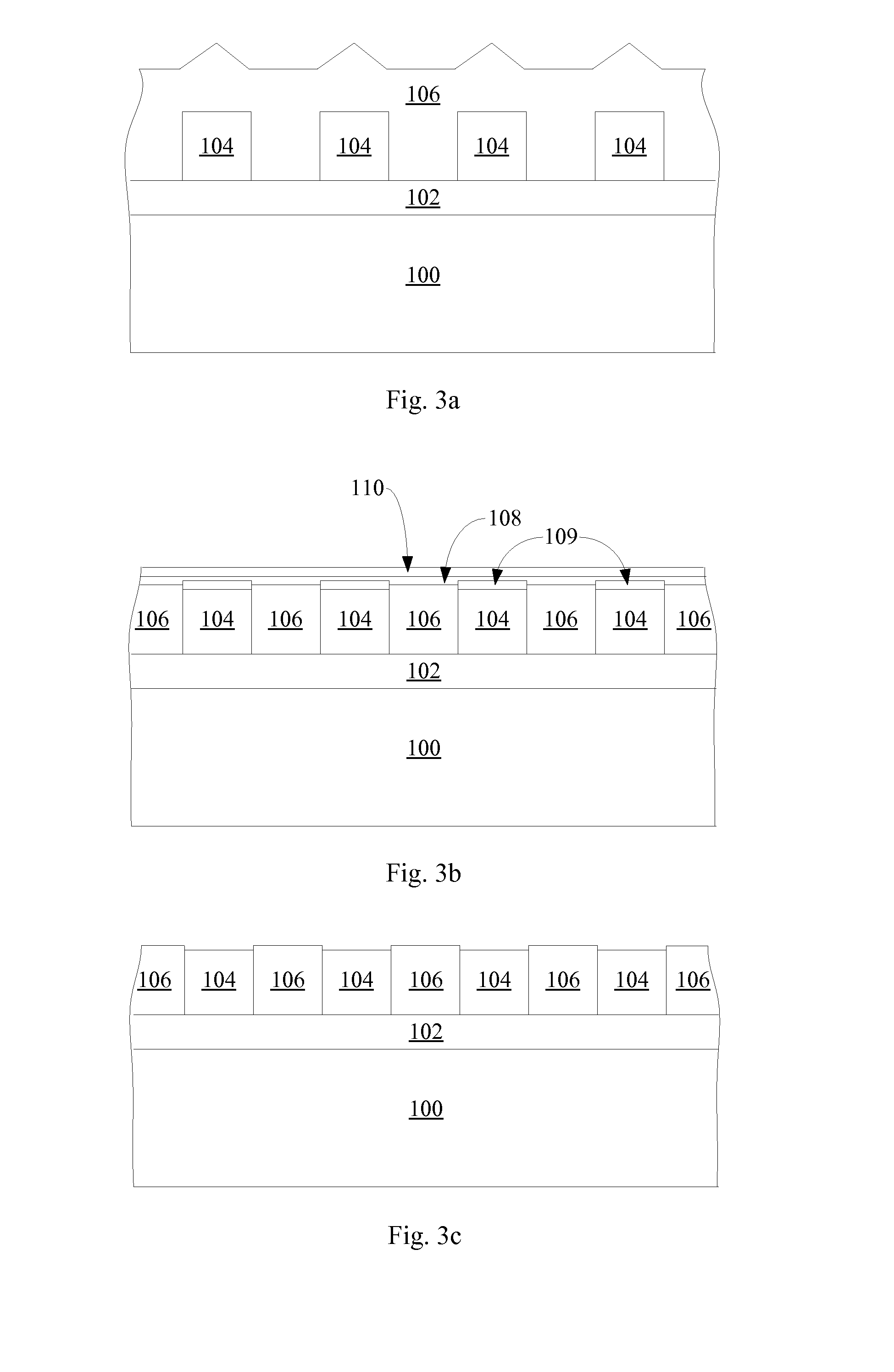
[0028]Turning to FIG. 3a, fabrication of the memory begins with a suitable substrate 100, for example a monocrystalline semiconductor material such as a conventional silicon wafer. An insulating layer 102 is formed over the substrate 100. Support circuitry, such as decoders and sense amplifiers, may be formed in the substrate before the memory is formed. In alternative embodiments, other substrates, such as silicon-on-insulator, glass, metal, or plastic, may be used instead.

[0029]A layer of silicon 104 is deposited on insulating layer 102 by any conventional method, for example by a chemical vapor deposition (CVD) method such as LPCVD. (For simplicity, this description will speak of the use of silicon for layer 104. It will be understood, however, that other semiconductor materials, preferably germanium or silicon-germanium alloys, may be used instead.) Silicon layer 104 may be any suitable thickness, for example between about 500 and about 4000 angstroms thic...

second embodiment

Bipolar Junction Transistor

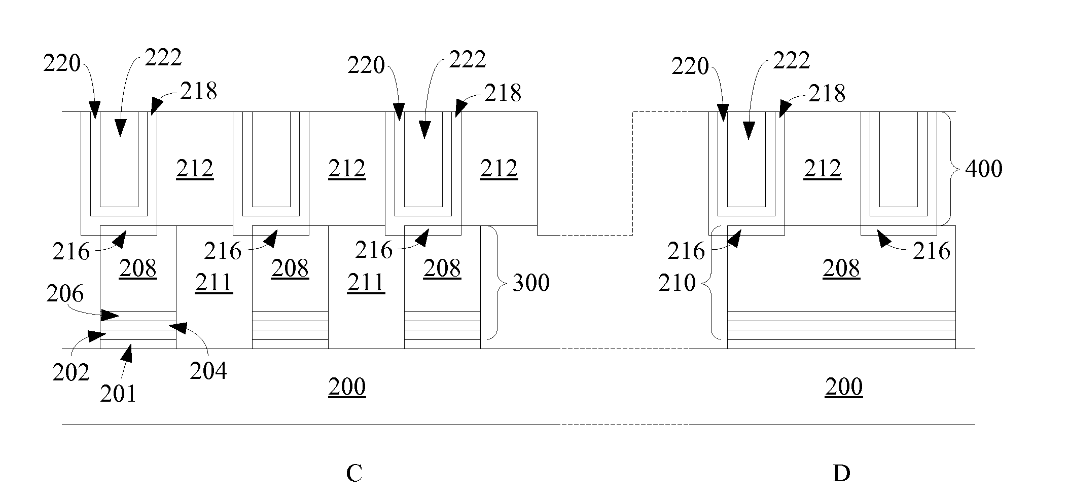
[0049]An alternative embodiment will be described in which a bipolar junction transistor is formed having its base in deposited silicon crystallized in contact with a silicide, preferably titanium silicide. In the example to be described, the bipolar junction transistors serve as switching elements in a monolithic three dimensional memory array in which each memory cell comprises a vertically oriented p-i-n diode paired with a dielectric rupture antifuse. Fabrication of an array of such memory cells is described in Herner, U.S. patent application Ser. No. 11 / 560,283, “Method for Making a P-I-N Diode Crystallized Adjacent to a Silicide in Series with A Dielectric Antifuse,” filed Nov. 15, 2006 and hereby incorporated by reference. Fabrication of this array including bipolar junction transistors as switching devices is described in more detail in Petti et al., the related application filed on even date herewith. To avoid obscuring the invention, not all of t...


PUM


Abstract

A method is described for forming a thin film transistor having its current-switching region in polycrystalline semiconductor material which has been crystallized in contact with titanium silicide, titanium silicide-germanide, or titanium germanide. The titanium silicide, titanium silicide-germanide, or titanium germanide is formed having feature size no more than 0.25 micron in the smallest dimension. The small feature size tends to inhibit the phase transformation from C49 to C54 phase titanium silicide. The C49 phase of titanium silicide has a very close lattice match to silicon, and thus provides a crystallization template for the silicon as it forms, allowing formation of large-grain, low-defect silicon. Titanium does not tend to migrate through the silicon during crystallization, limiting the danger of metal contamination. In preferred embodiments, the transistors thus formed may be, for example, field-effect transistors or bipolar junction transistors.

Description

RELATED APPLICATIONS[0001]This application is related to Petti et al., U.S. patent application Ser. No. ______, “Polycrystalline Thin Film Bipolar Transistors,” (Atty. Docket No. 2052 / 98694); and Petti et al., U.S. patent application Ser. No. ______, “Method for Forming Polycrystalline Thin Film Bipolar Transistors,” (Atty Docket No. 2052 / 99361) both filed on even date herewith and hereby incorporated by reference in their entirety.BACKGROUND OF THE INVENTION[0002]In general the performance of thin film transistors is impeded by grain boundaries and crystal defects in the semiconductor material in which the current-switching region of the transistor is formed.[0003]It is known to use metal catalysts to enhance grain size, but metals may contaminate the crystallized semiconductor material, damaging or ruining the device.[0004]It would be advantageous to enhance grain size and reduce defects in polycrystalline semiconductor material in which the current-switching region of a thin film...

Claims


Application Information

Patent Timeline
IPC IPC(8): H01L21/336H01L21/331
CPCH01L21/8221H01L27/0688H01L27/115H01L27/11521H01L27/11568H01L27/11578H01L27/1277H01L27/24H01L29/6675H01L29/66825H01L29/66833H01L29/7881H01L29/792H01L27/12H10B63/00H10B43/20H10B43/30H10B69/00H10B41/30
Inventor HERNER, S. BRADPETTI, CHRISTOPHER J.
Owner SANDISK TECH LLC
Why Eureka
Try Eureka