High resolution plasma etch

Active Publication Date: 2008-12-25
FEI CO
View PDF34 Cites 54 Cited by
  • Summary
  • Abstract
  • Description
  • Claims
  • Application Information

AI Technical Summary

Problems solved by technology

Lithography process are time consuming and, while efficient for processing a complete wafer, are less useful for localized processing.
While being able to form extremely precise structures, processing by such beams is typically too slow to be used for mass production of fine structures.
Many problems still exist, however, with the methods of fabrication as currently used and described above.
For example, it is difficult to precisely fabricate high aspect rati

Method used


Image

  • High resolution plasma etch
  • High resolution plasma etch
  • High resolution plasma etch

Examples


Embodiment Construction

[0017]Although those of ordinary skill in the art will readily recognize many alternative embodiments, especially in light of the examples provided herein, this detailed description is exemplary of a preferred embodiment of the present invention, the scope of which is limited only by the claims appended hereto.

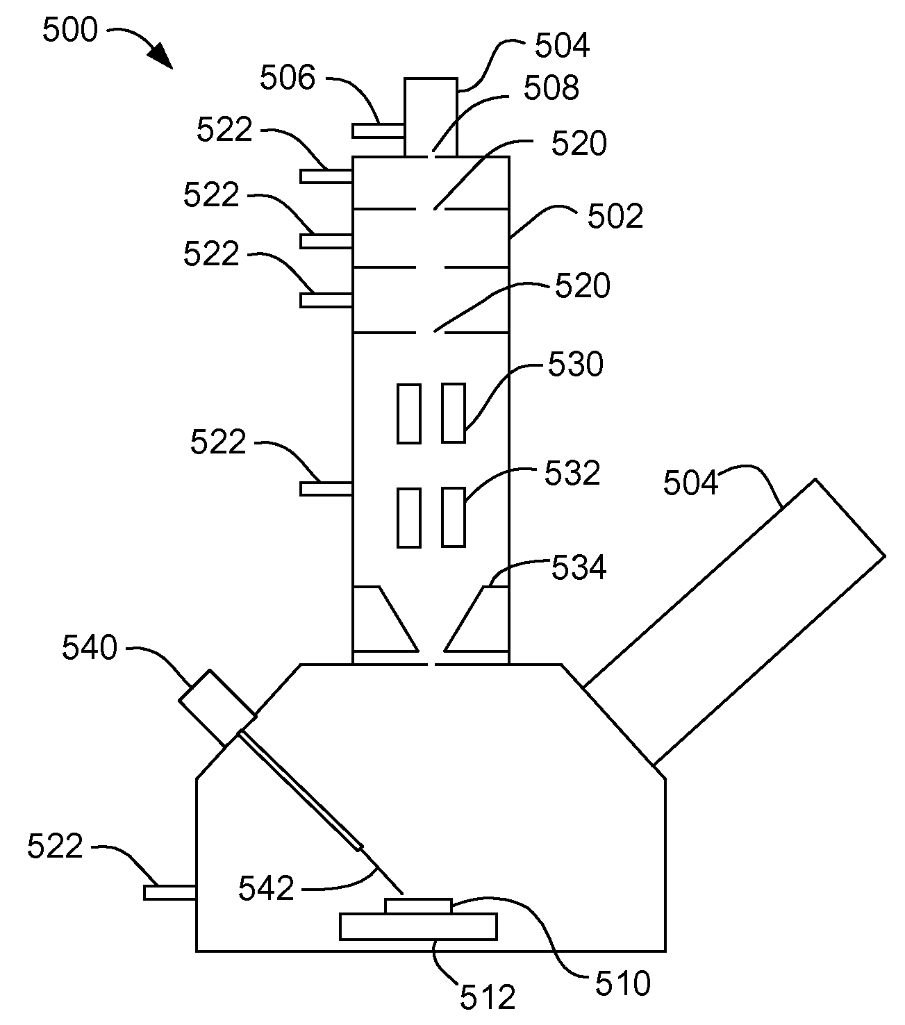
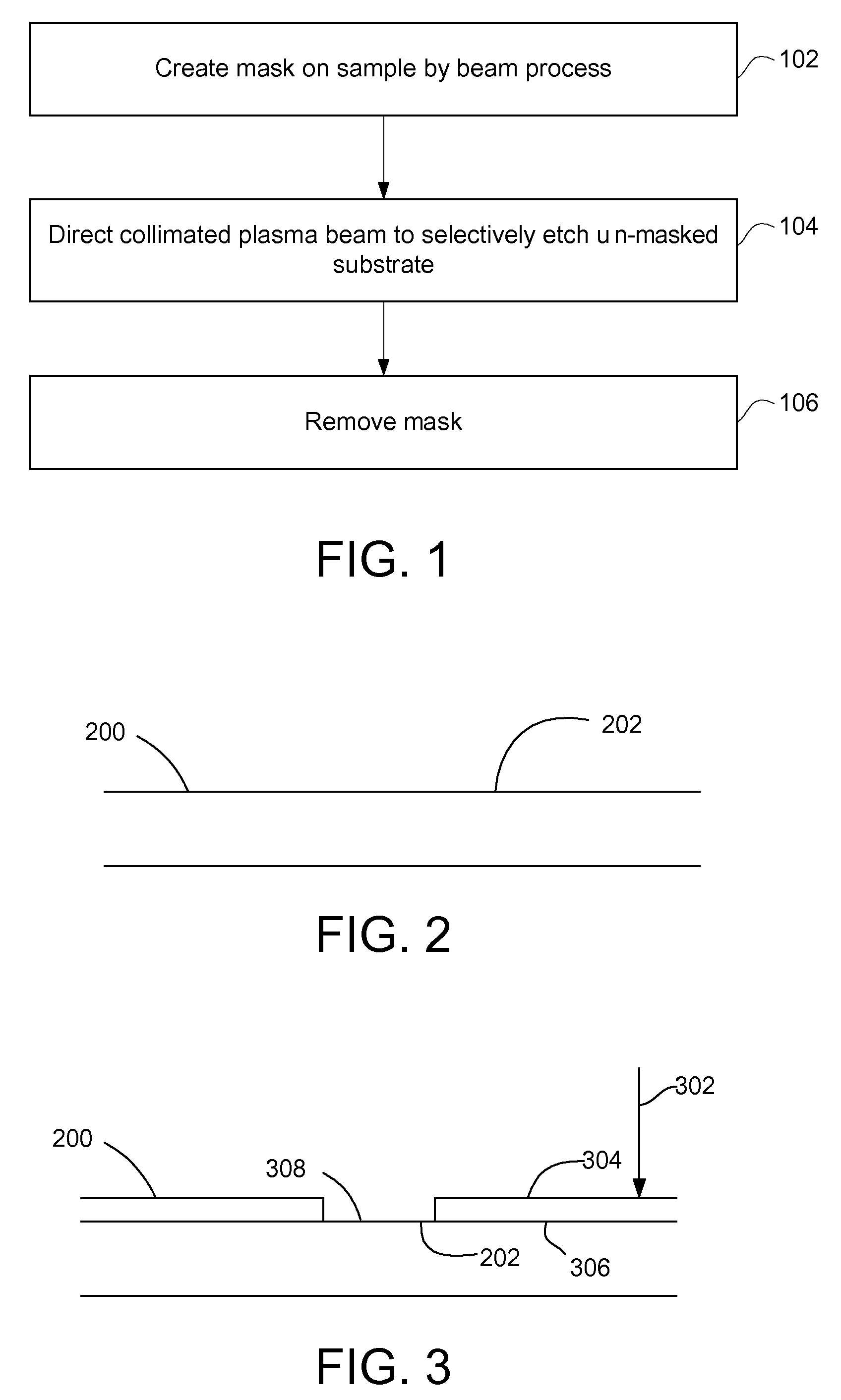
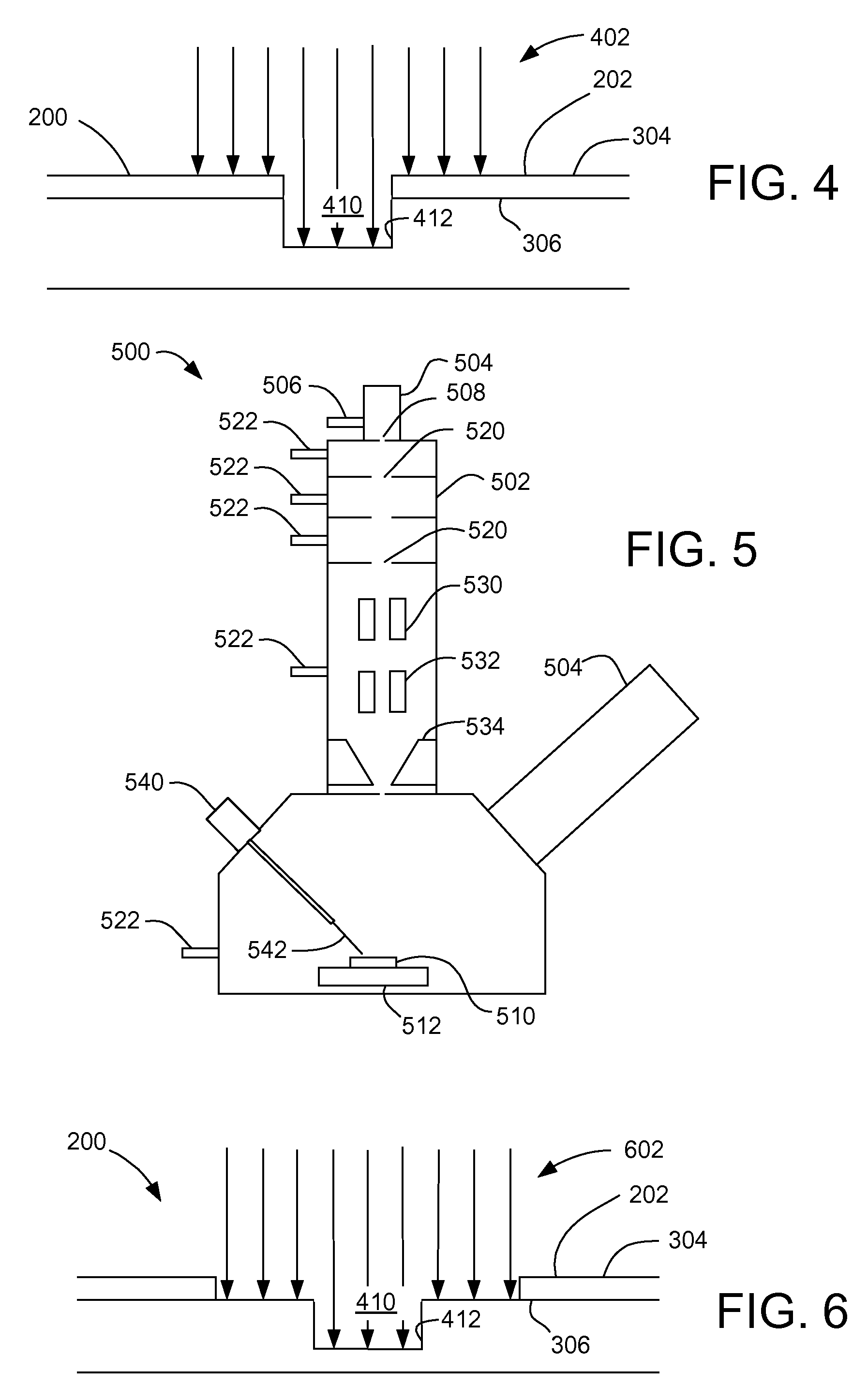
[0018]Preferred embodiments of the invention relate to a method for fabricating nanoscopic and microscopic structures, such as integrated circuits or micro-electromechanical systems, by a beam used to locally fabricate a protective mask, followed by use of a plasma beam etch process.

[0019]Where lithography is typically used for pattern definition in micromachining, beam processes as used in preferred embodiments of the present invention create precisely defined protective mask patterns on a substrate surface and, when followed by etching using a plasma beam, contribute to superior structural tolerances and machining flexibility. For example, beam deposition can produce surface...


PUM

PropertyMeasurementUnit
Energyaaaaaaaaaa
Energyaaaaaaaaaa
Diameteraaaaaaaaaa

Abstract

A method for fabrication of microscopic structures that uses a beam process, such as beam-induced decomposition of a precursor, to deposit a mask in a precise pattern and then a selective, plasma beam is applied, comprising the steps of first creating a protective mask upon surface portions of a substrate using a beam process such as an electron beam, focused ion beam (FIB), or laser process, and secondly etching unmasked substrate portions using a selective plasma beam etch process. Optionally, a third step comprising the removal of the protective mask may be performed with a second, materially oppositely selective plasma beam process.

Description

TECHNICAL FIELD OF THE INVENTION[0001]The present invention relates to materials processing on a microscopic scale.BACKGROUND OF THE INVENTION[0002]Modern technology demands the fabrication of ever smaller and more precise structures for electronic circuits, optical components, micro electromechanical structures (MEMS), and other applications. Many such structures and devices, on the scale of micrometers or nanometers, are fabricated on silicon wafers using photolithographic methods.[0003]A typical photolithography technique involves depositing a thin layer of a photosensitive material called a “photoresist” onto the surface of a semiconductor substrate such as a silicon wafer, by a process called “casting.” Photolithographic imaging is then used to transfer a desired pattern, designed on a photolithographic mask, to the photoresist by selective exposure to a radiation source such as light. The photoresist is then chemically developed to remove the radiation exposed areas (in a posi...

Claims


Application Information

Patent Timeline
IPC IPC(8): H01L21/3065
CPCB81C1/00531B81C2201/0132B81C2201/0143H01J37/3053H01J37/317H01J2237/3174H01J2237/31744H01J2237/31749B05C21/005
Inventor TOTH, MILOSSMITH, NOEL
Owner FEI CO
Why Eureka
Try Eureka