Electron gun, electron beam exposure apparatus, and exposure method

a technology of electron beam and exposure method, which is applied in the field of electron beam exposure apparatus and exposure method, can solve the problems of difficult uniform irradiation, deterioration in throughput, and complicated control but, and achieve the effect of avoiding melting or breaking

Active Publication Date: 2008-12-25
ADVANTEST CORP +1
View PDF5 Cites 19 Cited by
  • Summary
  • Abstract
  • Description
  • Claims
  • Application Information

AI Technical Summary

Benefits of technology

[0013]The present invention has been made in view of the aforementioned problem of the conventional technology. An object of the present invention is to provide an electron gun which is capable of reducing a quantity of sublimation attributable to heat from an electron source for emitting electrons and thereby allowing stable use for a longer period of time, and to provide an electron beam exposure apparatus and an exposure method using this electron gun.
[0017]In the present invention, only the electron emission surface at the tip of a chip as an electron generating material is exposed while the remaining side surface part is covered with the different material. When LaB6 is applied to the electron generating material, this different material is carbon (C), for example. Since the electron gun is operated at a low temperature, the chip hardly sublimates. In this way, the electron gun can be used stably for a long period of time while avoiding deformation of the electron emission surface. Moreover, as the side surface of the chip is covered with carbon, no electrons are emitted from the side surface of the chip even if an intense electric field is applied. Accordingly, a change in the shape of an electron beam can be avoided and a phenomenon of degradation in vacuum attributable to a rise in temperature of an unwanted part can be prevented. Not only the side surface is covered, but also the entire chip is preferably covered except the electron emission part on the tip with a protective film. This configuration is effective, not in terms of the electron emission, but in terms for suppressing sublimation and reducing an amount of an attached material onto a Wehelt cylinder.
[0019]In the present invention, the electric potential at the extraction electrode is set lower than the electric potential at the electron source prior to performing the exposure. In this way, no electrons are extracted from the electron source. Accordingly, the electron source can be avoided from melting or breakage when conditioning is carried out.

Problems solved by technology

An increase in exposure time to supplement the weakened electron beam due to the change over time may lead not only to complication of control but also to deterioration in the throughput.
Accordingly, such deformation makes the uniform irradiation difficult, of a variable rectangular beam or a block pattern beam which causes the intensity reduction of the emitted electron beam.
Occurrence of this micro discharge may cause instabilities of the electron beam quantity and of a radiating position, thereby being unable to use an electron beam exposure apparatus properly.
Moreover, the throughput may be deteriorated due to the time consumption for adjustment or other operations.
The most serious problem is that the pattern drawn during the occurrence of the micro discharge may lead a loss of reliability.
Hei 8-184699, discloses the technique to suppress depletion of the chip by covering the surface of the chip with the two-layer structure made of tungsten (W) and rhenium (Re), this technique is unable to prevent the change in the shape of a chip attributable to sublimation of an electron emission surface not covered with the two-layer structure.

Method used


Image

  • Electron gun, electron beam exposure apparatus, and exposure method
  • Electron gun, electron beam exposure apparatus, and exposure method
  • Electron gun, electron beam exposure apparatus, and exposure method

Examples


Embodiment Construction

[0027]Now, embodiments of the present invention will be described blow with reference to the accompanying drawings.

[0028]First of all, a configuration of an electron beam exposure apparatus will be described. Subsequently, a configuration of an electron gun will be described and then a configuration of an electron source in the electron gun, which constitutes a characteristic part of the present invention, will be described. Next, an exposure method for an exposure apparatus applying the electron gun of the present invention will be described. After that, a method of forming a region for controlling electron emission on a surface of the electron source will be described. Lastly, effects of using the electron gun of the embodiment of the present invention will be described.

(Configuration of Electron Beam Exposure Apparatus)

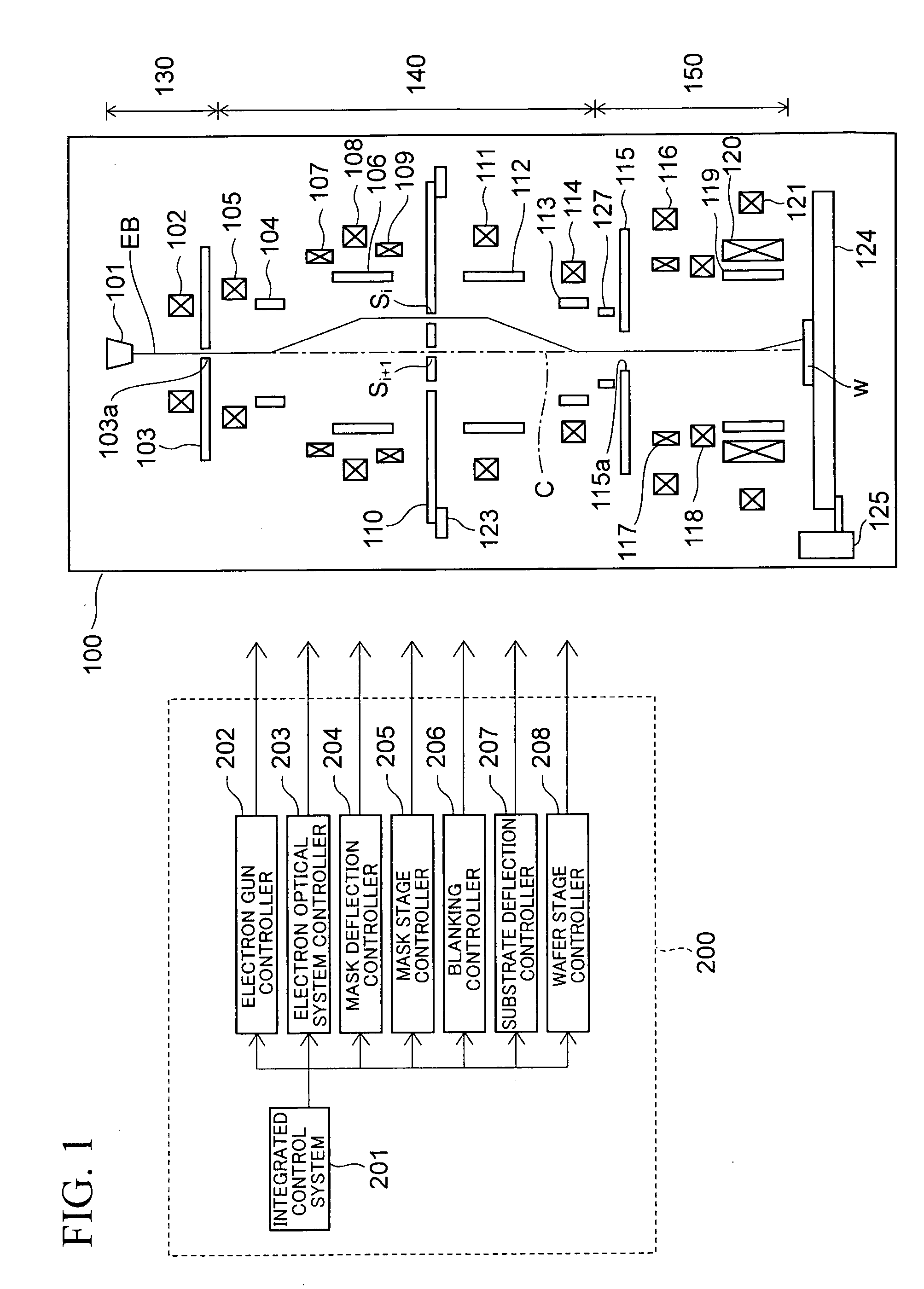
[0029]FIG. 1 is a block diagram of an electron beam exposure apparatus according to an embodiment of the present invention.

[0030]The electron beam exposure apparat...


PUM


Abstract

An electron gun includes an electron source configured to emit electrons. The electron source includes an electron emission region configured to emit the electrons and an electron emission restrictive region configured to restrict emission of the electrons. The electron emission restrictive region is located on a side surface of the electron source except an electron emission surface on a tip of the electron source and is covered with a different material from the electron source. The electron gun emits thermal field-emitted electrons by applying an electric field to the tip while maintaining a sufficiently low temperature to avoid sublimation of a material of the electron source. The material of the electron source may be lanthanum hexaboride (LaB6) or cerium hexaboride (CeB6). The electron emission restrictive region may be covered with carbon.

Description

CROSS-REFERENCE TO RELATED APPLICATIONS[0001]This application is a continuation of prior International Patent Application No. PCT / JP2006 / 321991, filed Nov. 2, 2006, the entire contents of which are incorporated herein by reference.BACKGROUND OF THE INVENTION[0002]1. Field of the Invention[0003]The present invention relates to an electron gun used in a lithography process for manufacturing a semiconductor device, an electron beam exposure apparatus provided with the electron gun, and an exposure method.[0004]2. Description of the Prior Art[0005]In order to enhance throughput, a recent electron beam exposure apparatus is provided with a mask having a variable rectangular aperture formed therein, or with multiple mask patterns. One of the mask patterns is firstly selected by means of beam deflection, and the selected pattern is then transferred onto a wafer through exposure. An exposure method employing the above-mentioned multiple mask patterns is achieved by an electron beam exposure...

Claims


Application Information

Patent Timeline
Patent Type & Authority Applications(United States)
IPC IPC(8): H01J3/02
CPCH01J37/073H01J2237/06316H01J2237/06341H01J2237/3175
Inventor YASUDA, HIROSHIHARAGUCHI, TAKESHIOOAE, YOSHIHISASATOH, TAKAMASATERUI, YOSHINORISAKAWA, SEIICHINONOGAKI, RYOZO
Owner ADVANTEST CORP
Why Eureka
Try Eureka