
Array molded package-on-package having redistribution lines

a technology of assembly and package, applied in the direction of manufacturing tools, basic electric elements, metal working apparatus, etc., can solve the problems of inability to meet the requirements of production, so as to improve the testability and thus yield, simplify the fabrication method, and shorten the time-to-market

Active Publication Date: 2008-12-25
TEXAS INSTR INC
View PDF17 Cites 154 Cited by
  • Summary
  • Abstract
  • Description
  • Claims
  • Application Information

AI Technical Summary

Benefits of technology

The invention is a versatile mold that allows for the production of semiconductor devices with flexible interconnection options for package-on-package methods. The mold has exchangeable device-specific inserts that provide low-cost, simplified fabrication methods and improved testability and yield. The invention also provides a method for fabricating a semiconductor device with surface grooves for electrical routing, allowing for the coupling of semiconductor devices to form a package-on-package assembly. The technical effects of the invention include improved flexibility, reduced warping, and high product reliability.

Problems solved by technology

These expectations tend to run quickly into difficulties for various reasons.
The thickness of the package-on-package products as the simple sum of the thicknesses of the semiconductor chips, electric interconnections, and encapsulations is often unacceptably large, especially for hand-held wireless equipments.
In contrast, when the thickness is reduced, the products run increasingly into warpage problems caused by the mismatch in the coefficients of thermal expansion (CTE) between the semiconductor chip, the plastic substrates, the molding compound, the solder balls, and the printed circuit board.
Warpage can lead to some of the most debilitating problems encountered by semiconductor assemblies such as the fracture and separation of solder joints, or the separation of materials followed by moisture ingress.
In addition, the selection of partners for package-on-package products is often limited because their electrical interconnection has to be customized and may require additional metal levels.

Method used


Image

  • Array molded package-on-package having redistribution lines
  • Array molded package-on-package having redistribution lines
  • Array molded package-on-package having redistribution lines

Examples


Embodiment Construction

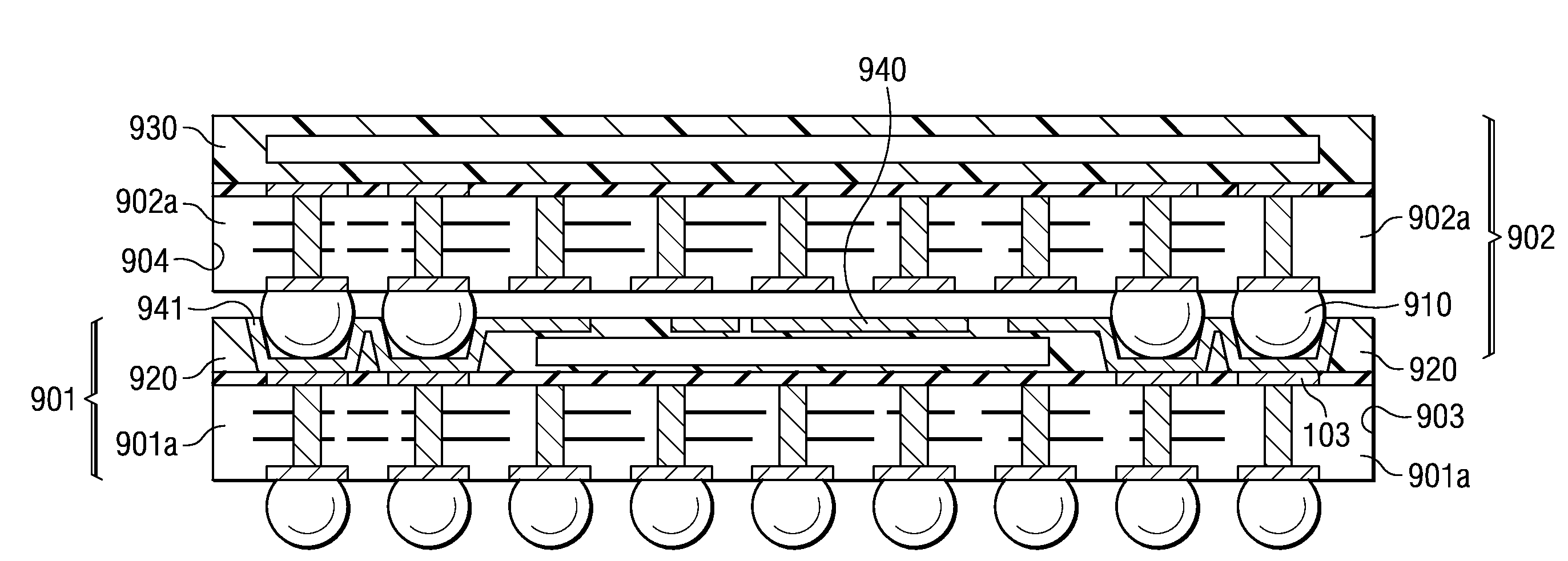
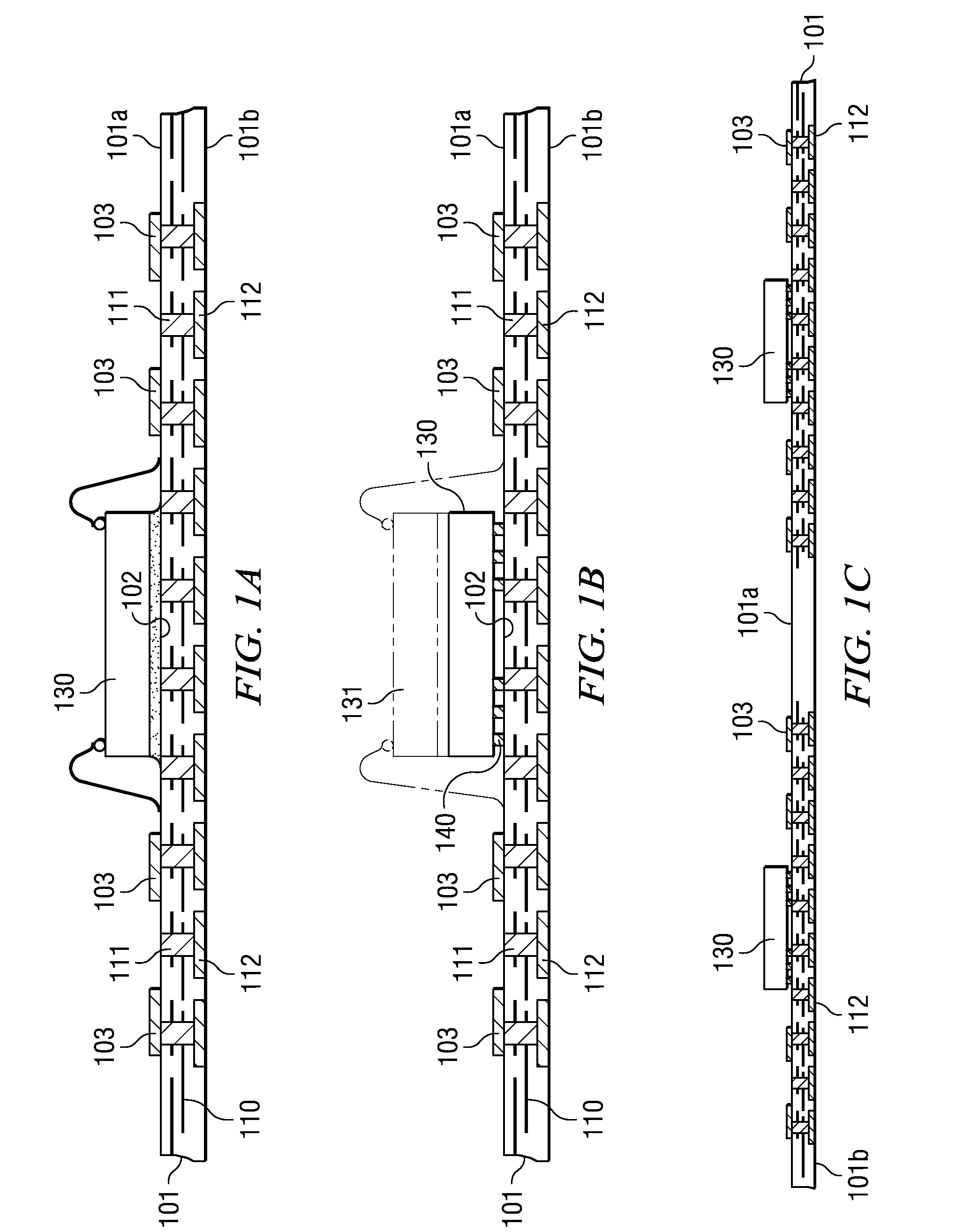
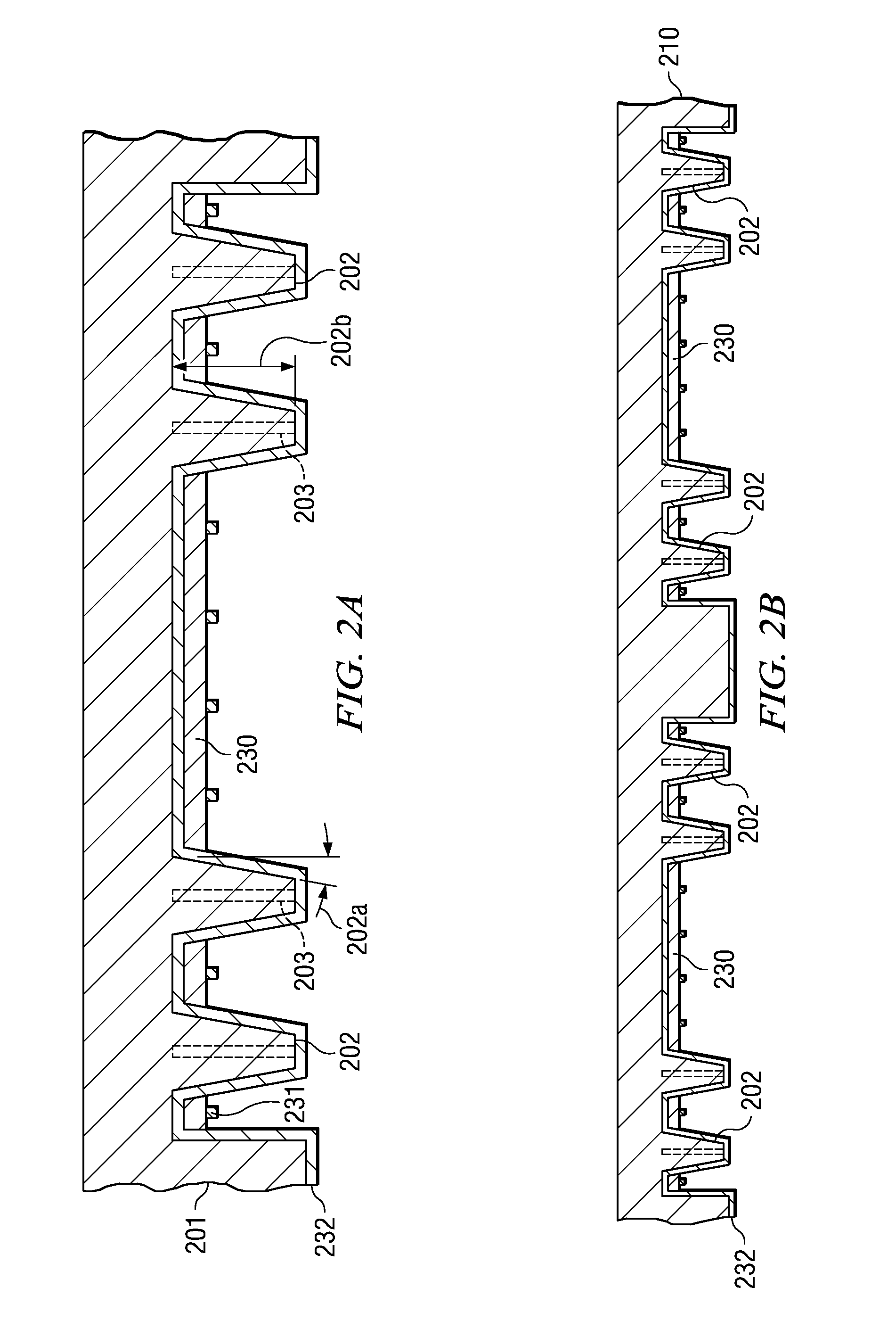
[0032]FIGS. 1A through 7 illustrate schematically the steps of one embodiment of the present invention, a method for array-molding semiconductor devices. The steps shown in FIGS. 1A and 1B show the attachment and assembly of a semiconductor chip on a substrate by wire bonding (FIG. 1A) and by flip-chip technology (FIG. 1B); FIG. 1C exemplifies a portion of an array of chips attached by flip-chip. A sheet-like substrate 101 with insulating core (for example, plastic, glass-fiber reinforced, ceramic) is integral with two or more patterned layers of conductive lines and conductive vias (preferably copper) and contact pads in pad locations (lines 110 do not reach beyond the boundaries of substrate 101). Substrate 101 has a first surface 101a and a second surface 101b, and a preferred thickness range from 0.05 to 0.5 mm. The first surface 101a includes chip assembly sites 102 and contact pads 103 in pad locations. The metal of the contact pads is preferably copper with a solderable surfa...


PUM

PropertyMeasurementUnit
distanceaaaaaaaaaa
distanceaaaaaaaaaa
heightaaaaaaaaaa

Abstract

A semiconductor device with a sheet-like insulating substrate (101) integral with two or more patterned layers of conductive lines and vias, a chip attached to an assembly site, and contact pads (103) in pad locations has an encapsulated region on the top surface of the substrate, extending to the edge of the substrate, enclosing the chip, and having contact apertures (703) at the pad locations for external communication with the pad metal surfaces. The apertures may have not-smooth sidewall surfaces and may be filled with solder material (704) to contact the pads. Metal-filled surface grooves (710) in the encapsulated region, with smooth groove bottom and sidewalls, are selected to serve as customized routing interconnections, or redistribution lines, between selected apertures and thus to facilitate the coupling with another semiconductor device to form a package-on-package assembly.

Description

FIELD OF THE INVENTION[0001]The present invention is related in general to the field of semiconductor devices and processes and more specifically to the structure and fabrication method of low-profile, vertically integrated package-on-package integrated circuit assemblies having redistribution lines.DESCRIPTION OF THE RELATED ART[0002]Today's package-on-package semiconductor devices enjoy increasing popularity, because they promise to use components already developed and thus quickly available, they are supposed retain a slim space-saving contour after assembly, and they are expected to be robust in terms of reliability in use-test under variable temperature and moisture conditions. These expectations tend to run quickly into difficulties for various reasons.[0003]The thickness of the package-on-package products as the simple sum of the thicknesses of the semiconductor chips, electric interconnections, and encapsulations is often unacceptably large, especially for hand-held wireless...

Claims


Application Information

Patent Timeline
Patent Type & Authority Applications(United States)
IPC IPC(8): H01L23/12B22D19/08H01L21/50
CPCH01L21/561H01L21/565H01L23/3128H01L23/49816H01L23/49827H01L23/49833H01L24/97H01L2224/16225H01L2224/32225H01L2224/48225H01L2224/48227H01L2224/73265H01L2224/97H01L2924/01013H01L2924/01029H01L2924/01032H01L2924/01079H01L2924/01082H01L2924/09701H01L2924/15311H01L24/48H01L2924/01005H01L2924/01006H01L2924/01033H01L2924/014H01L2224/48465H01L2224/48091Y10T29/5317H01L2224/81H01L2224/85H01L2924/00H01L2224/32145H01L2924/00012H01L2924/00014H01L24/73H01L2224/48472H01L2924/14H01L2924/181H01L2924/1815H01L2224/45099H01L2224/45015H01L2924/207
Inventor GERBER, MARK A.WALTER, DAVID N.
Owner TEXAS INSTR INC
Learn More