Method for Manufacturing a Hybrid Microlens

Inactive Publication Date: 2008-12-25
KOREA INST OF IND TECH
View PDF1 Cites 7 Cited by
  • Summary
  • Abstract
  • Description
  • Claims
  • Application Information

AI Technical Summary

Benefits of technology

[0011]As described above, according to the present invention, hybrid microlenses can be manufactured with photoresists formed by means of vertical light exposure and slant light exposure through a reflow process. Thus, there are advantages in that a hybrid microlens array pattern can be manufactured through a simplified manufacturing process and production costs and time can be reduced.
[0012]In addition, the sizes and inclinations of photoresists can be controlled through light-exposing and reflow processes so that hybrid microlenses can be arbitrarily manufactured according to manufacturer's intention. Thus, there is an advantage in that hybrid microlenses with desired optical properties can be arbitrarily fabricated on a light guiding plate.

Problems solved by technology

Contrary to CRTs, PDPs and FEDs, a liquid crystal display is a non-luminescent device and thus cannot be used in a dark place without light.
However, the etched dot type has a problem in a wet etching process.
Thus, there are problems in that it is difficult to manufacture a pattern with a certain size or distance, it is difficult to optically control light due to an uneven etched surface, production time is extended and production costs increase.
In addition, even in the case of the diffusive ink dot type, an optical efficiency is significantly degraded due to absorption and scattering of a diffusive ink itself.
Thus, there is a problem in that an expensive prism film or diffusion film should be used to increase the emergence angle.
However, there is a problem in that since this pattern is formed through a mechanical process or an etching process, a uniform configuration cannot be easily achieved.

Method used


Image

  • Method for Manufacturing a Hybrid Microlens
  • Method for Manufacturing a Hybrid Microlens
  • Method for Manufacturing a Hybrid Microlens

Examples


Embodiment Construction

[0024]Hereinafter, preferred embodiments of the present invention will be described in detail with reference to the accompanying drawings.

[0025]In the following description, detailed explanation of known related functions and constitutions may be omitted to avoid unnecessarily obscuring the subject manner of the present invention.

[0026]Further, the terms used in the description are defined considering the functions of the present invention and may vary depending on the intention or usual practice of a user or operator. Therefore, the definitions should be made based on the entire contents of the description.

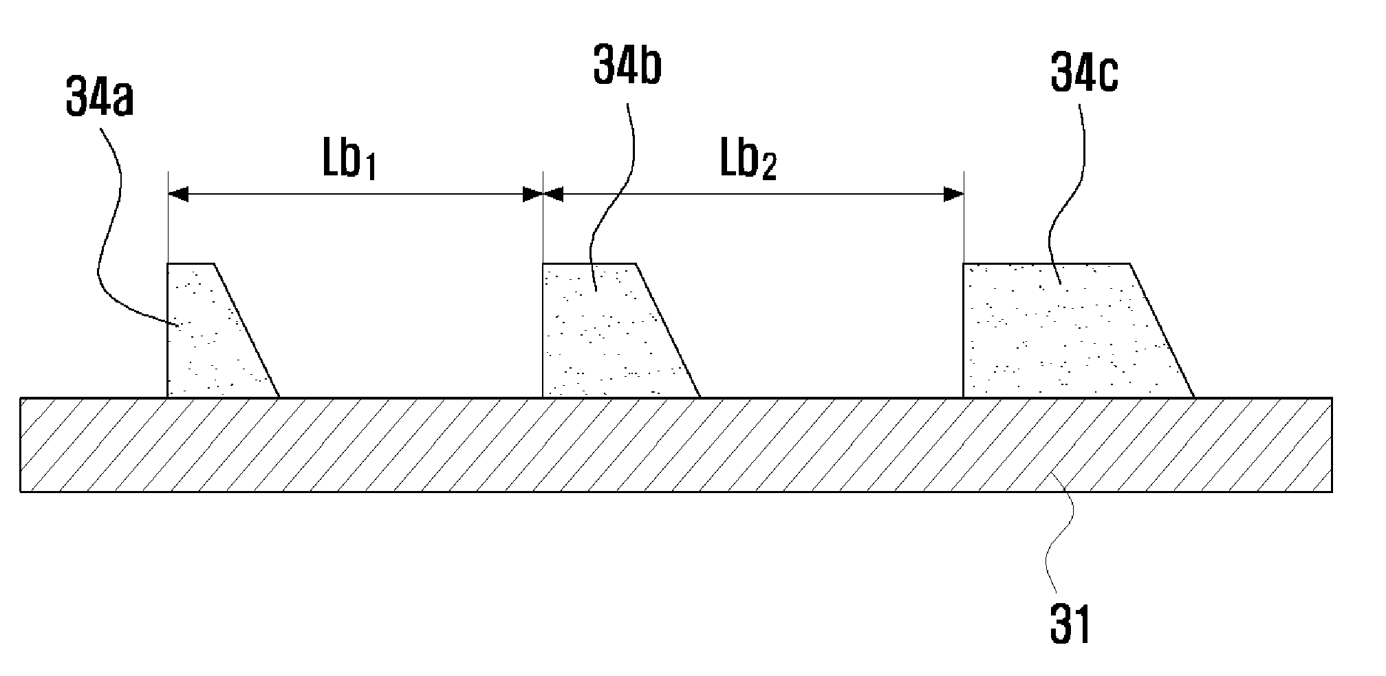
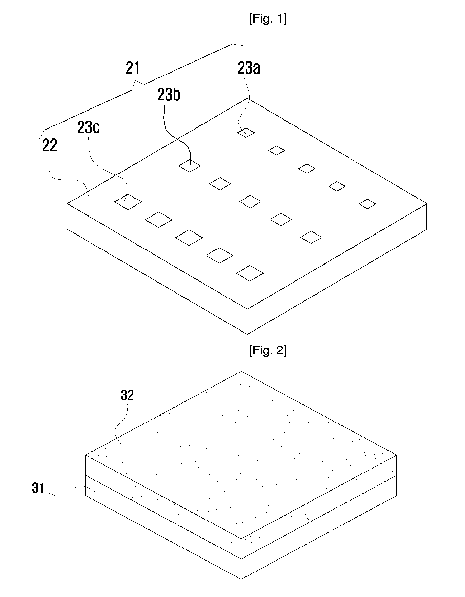
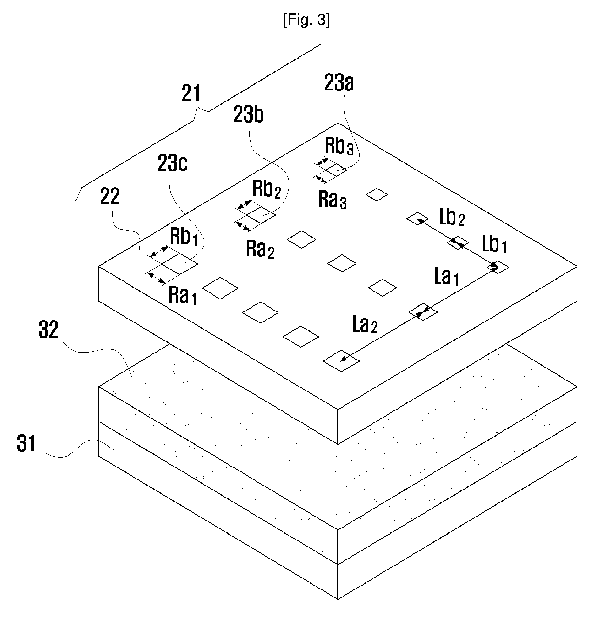
[0027]In the present invention, a mask 21 to be used for a light-exposing process is first fabricated, as shown in FIG. 1. Here, as for the mask, a film mask or a chromium mask may be used depending on the precision of a pattern. In case of the use of a chromium mask, the mask can be fabricated with a precision of about 1 .

[0028]FIG. 1 is a perspective view of a mask for use in t...


PUM


Abstract

The present invention provides a method for manufacturing hybrid microlenses of a light guiding plate using a semiconductor reflow process, comprising: a first step of aligning a mask on a substrate coated with a photoresist, wherein the mask is formed with a first region through which light can be transmitted and a plurality of second regions through which light cannot be transmitted, and the second regions have different sizes and shapes to form hybrid arrays; a second step of performing slant light exposure and vertical light exposure at least once in such a manner that light radiated from the top to the bottom of the second regions forming the hybrid arrays has an unsymmetrical inclination angle in at least one direction; a third step of developing the slant light-exposed substrate to obtain hybrid photoresist posts with various sizes and shapes; a fourth step of performing a reflow process to allow the hybrid photoresist posts to be curved so that a hybrid microlens pattern can be obtained; a fifth step of fabricating a depressed stamper with the hybrid microlens pattern engraved in a depressed fashion therein; and a sixth step of forming a light guiding plate by using the depressed stamper as a mold so that the hybrid microlens pattern can be formed in a raised pattern in the light guiding plate.

Description

TECHNICAL FIELD[0001]The present invention relates to a micro-pattern machining technology and a micro-molding technology, and more particularly, to a method for manufacturing hybrid microlenses for controlling light diffusion and dispersion and a viewing angle in a microlens array, a light guiding plate or the like, and a light guiding plate manufactured using the method.BACKGROUND ART[0002]In general, a backlight unit of a liquid crystal display (LCD) is used as an illumination device that provides light uniformly over an entire panel of the liquid crystal display, and the panel of the liquid crystal display properly controls the amount of light to be transmitted so that an image can be displayed thereon. Contrary to CRTs, PDPs and FEDs, a liquid crystal display is a non-luminescent device and thus cannot be used in a dark place without light.[0003]To solve such a disadvantage and allow a liquid crystal display to be used in a dark place, a backlight unit is used as an illuminatio...

Claims


Application Information

Patent Timeline
IPC IPC(8): G02B27/12G02B5/02G03F7/20
CPCG02B3/0018G02B3/0031G02B3/0043G02B3/005G02B6/0036G02B6/005G02B6/0061G02B6/0065A61B3/12A61B2560/04
Inventor HWANG, CHUL JINKIM, JONG SUNKO, YOUNG BAEHEO, YOUNG MOO
Owner KOREA INST OF IND TECH
Why Eureka
Try Eureka