Optical Scanning Device

a scanning device and optical technology, applied in the field of optical scanning devices, can solve the problems of large increase in the amount of spherical aberration, introduction of aberration, and spherical aberration, and achieve the effects of reducing the overall light path, optical scanning device even more compact, and optical scanning device more compa

Inactive Publication Date: 2008-12-25
KONINKLIJKE PHILIPS ELECTRONICS NV
View PDF16 Cites 2 Cited by
  • Summary
  • Abstract
  • Description
  • Claims
  • Application Information

AI Technical Summary

Benefits of technology

[0015]An advantage of the invention is that the use of a folding means makes it possible to reduce the overall light path by a factor of 2 and make the optical scanning device more compact than that known from prior art. In addition, said compensation module may be carried out with any SA compensation means be it an optical path length compensation means or a conjugate changing compensation means.
[0016]In a particular embodiment, said reflective means faces a beam splitter so as to reflect towards said information layer through said beam splitter the light path of said radiation beam coming out from said beam splitter.
[0017]Optical path length compensation means may be either a classical switching LC cell or a discrete step phase plate. In this latter case, a correction lens must be provided so as to ensure focusing of the radiation beam on the relevant phase step.
[0018]Due to the possible occurrence of coma effect associated with the optical path length compensation means, one may preferably use conjugate changing compensation means.
[0019]In a preferred embodiment, said conjugate changing compensation means comprises a SA correction lens. The advantage of this embodiment is to allow the use of SA correction lens having a short focal length leading to a short full stroke of the compensation means so making a compact light path geometry feasible. Furthermore, it should be noted that the numerical aperture is high in accordance with one goal of the invention. However, this feature is not detrimental to rim intensities insofar as the focal length of the SA correction lens does not influence the rim intensities, which are independently determined by the focal length of the collimator.
[0020]In order to make the optical scanning device even more compact, the invention provides that said optical device comprises detection means of an information detection beam, a grating being arranged in said information detection beam and said detection means being placed in the focal plane of said SA correction lens. Actually, this provision enables the detection means to be placed in the focal plane of the SA correction lens next to the reflecting means of the compensation module. Thus being integrated to the compensation module, the detection means do not take up more space that the compensation module itself.

Problems solved by technology

However, the numerical aperture of the radiation beam is relatively low resulting in an amount of spherical aberration within the tolerances of the optical scanning device, so that no spherical aberration compensation is needed.
Actually, the amount of aberration is proportional to the fourth power of the numerical aperture of the beam, which means that a slight increase in the numerical aperture leads to a large increase in the amount of spherical aberration.
As a consequence, the amount of aberration introduced when switching from one information layer to another is such increased that it needs to be compensated.
The drawbacks of this solution for SA compensation are: it is difficult to make for small pupil radii and intolerant to pupil displacement during radial tracking due to coma effect.
As a result, the LC cell should be attached to the tracking actuator which is difficult to carry out for small form factor optical drives, because the weight on the tracking actuator would deteriorate the system performance.
The drawback of this solution is that for regular light path geometries with collimator having focal lengths of several millimetres it results in a rather large collimator displacement, typically several millimetres in high numerical aperture light path, which again is difficult to carry out in a small form factor optical drive.

Method used


Image

  • Optical Scanning Device
  • Optical Scanning Device
  • Optical Scanning Device

Examples


Embodiment Construction

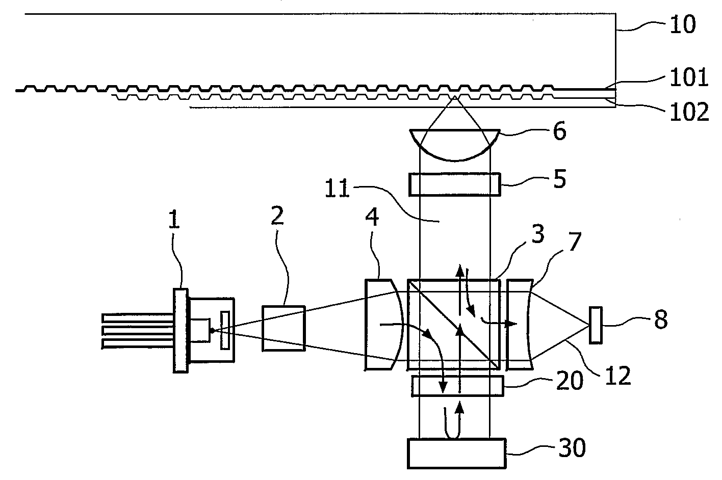
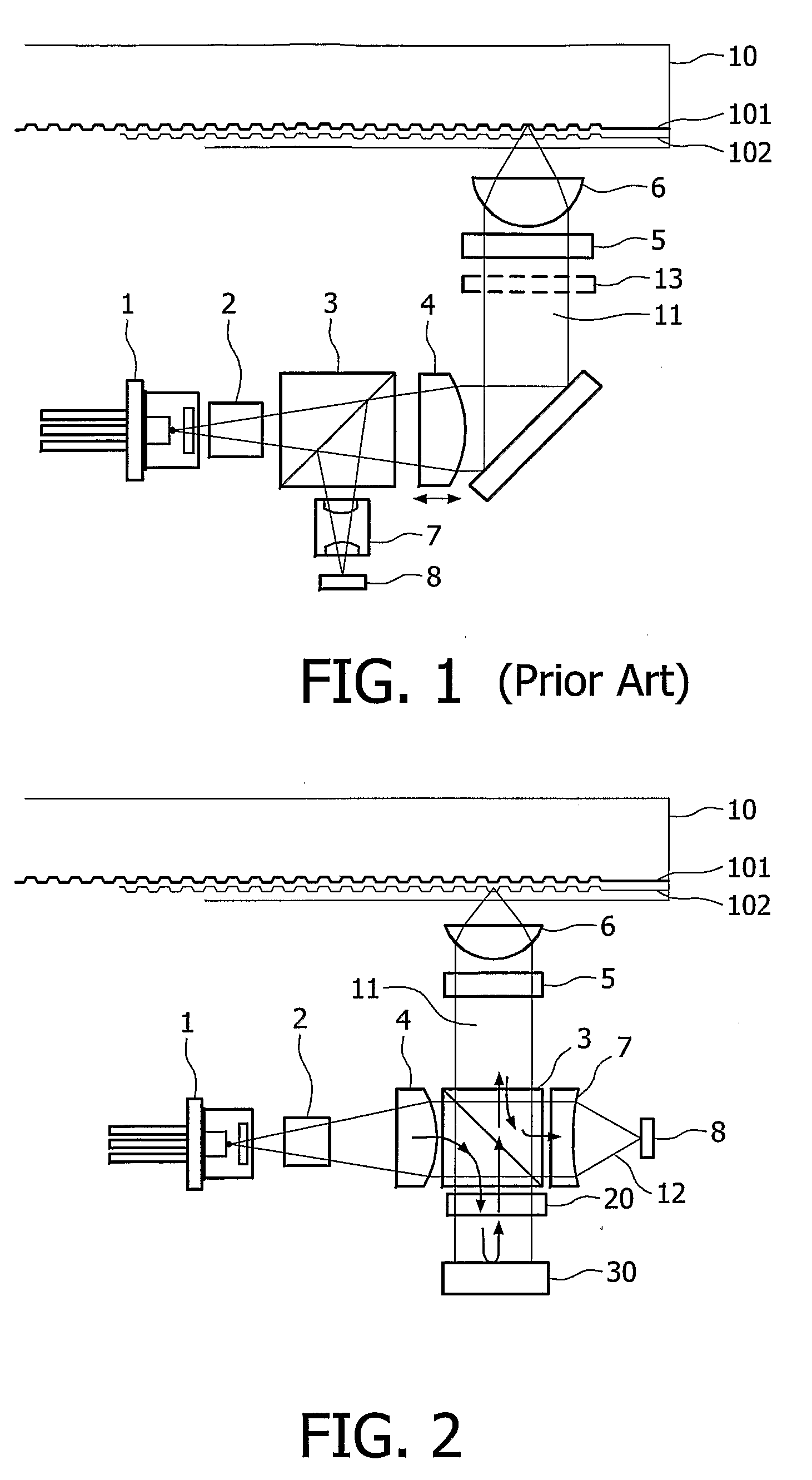
[0030]A general representation of an optical scanning device in accordance with the invention is depicted in FIG. 2.

[0031]In the embodiment shown in FIG. 2, such an optical scanning device is designed for scanning two information layers 101 and 102 in an information carrier, 10. The information carrier 10 may of course have more than two information layers and even only one when the optical scanning device is incorporated in players and recorders compatible with CD, DVD and BD formats for instance.

[0032]The optical scanning device of FIG. 2 comprises a radiation source 1, a laser diode for example, for producing a radiation beam 11 intended to be focused on said information layers 101 and 102. The light emitted by the radiation source 1 passes through an optional beam shaper 2, a collimator 4 for producing a parallel radiation beam, and a polarising beam splitter 3. Focusing of the radiation beam 11 on the information carrier 10 is performed by an objective lens 6 which is controlle...


PUM

PropertyMeasurementUnit
focal lengthaaaaaaaaaa

Abstract

The invention relates to an optical scanning device for scanning at least one information layer (101, 102) in an information carrier (10), comprising means (1) for generating a radiation beam (11) intended to be focused on the information layer (101, 102). A spherical aberration (SA) compensation module (40) is arranged in the light path of the radiation beam (11) and comprises a SA compensation means (41) and a reflective means (42) for folding the light path of the radiation beam (11).

Description

FIELD OF THE INVENTION[0001]The present invention relates to an optical scanning device for scanning at least one information layer in an information carrier.[0002]The invention is particularly relevant to any optical disc apparatus for reading and / or recording data from and / or to at least one information layer carried by the optical disc. Such optical disc apparatus may be a CD (Compact Disc), a DVD (Digital Versatile Disc) or a BD (Blu-Ray Disc) player and / or recorder.BACKGROUND OF THE INVENTION[0003]Information carriers having a plurality of information layers are widely used. For example, certain DVDs comprise a first and a second information layer which can be scanned by means of a radiation beam intended to be focused on one of the information layers in order to read from or record to the selected information layer. The expression “scanning” means either reading or writing data from or to an information layer.[0004]An optical scanning device for scanning such a dual-layer DVD ...

Claims


Application Information

Patent Timeline
Patent Type & Authority Applications(United States)
IPC IPC(8): G11B7/00G11B7/135
CPCG11B7/1362G11B7/13925G11B7/13927G11B2007/0013G11B7/1367G11B7/1369G11B7/1378G11B7/1392
Inventor SCHLEIPEN, JOHANNES JOSEPH HUBERTINA BARBARA
Owner KONINKLIJKE PHILIPS ELECTRONICS NV
Why Eureka
Try Eureka