Optical switch and fabrication method thereof

An optical switch and manufacturing method technology, applied in optics, optical components, manufacturing tools, etc., can solve the problems of reducing the accuracy of etching patterns, rough sidewalls of micro mirrors, increasing etching masks, etc.

Inactive Publication Date: 2005-07-13
SAMSUNG ELECTRO MECHANICS CO LTD
View PDF0 Cites 5 Cited by
  • Summary
  • Abstract
  • Description
  • Claims
  • Application Information

AI Technical Summary

Problems solved by technology

However, etching at a high etch rate poses a serious problem, that is, the sidewalls of the micromirrors are gradually roughened in proportion to the etch rate and exposed to the reactive gas for a long time, thereby being damaged.
Another problem is that in order to etch the lower etch rate actuating elements, the etch mask is required to be thick and hard to withstand the long etch time and high etch rate processing conditions
[0011] If the etch mask is not thick or hard enough, the etched area will not maintain its shape under high etch rate and long etch time processing conditions, so that the desired structure cannot be formed
However, increasing the thickness and hardness of the etch mask also limits the selectivity of the etch mask and reduces the accuracy of the etched pattern

Method used


Image

  • Optical switch and fabrication method thereof
  • Optical switch and fabrication method thereof
  • Optical switch and fabrication method thereof

Examples


Embodiment Construction

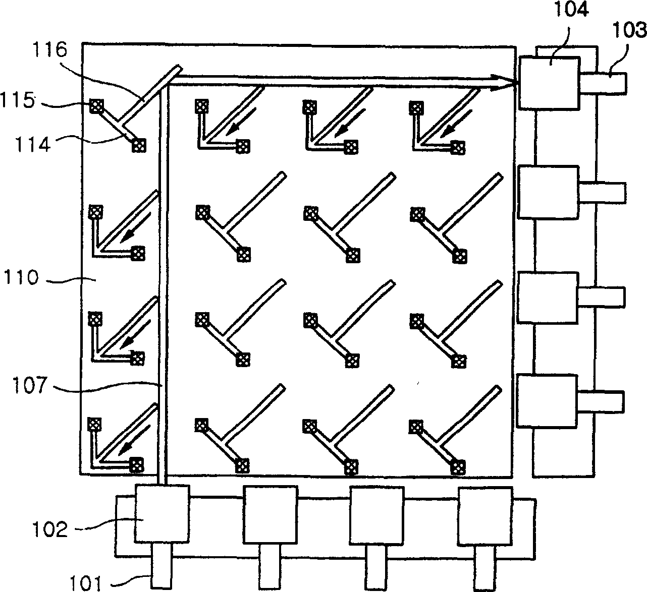
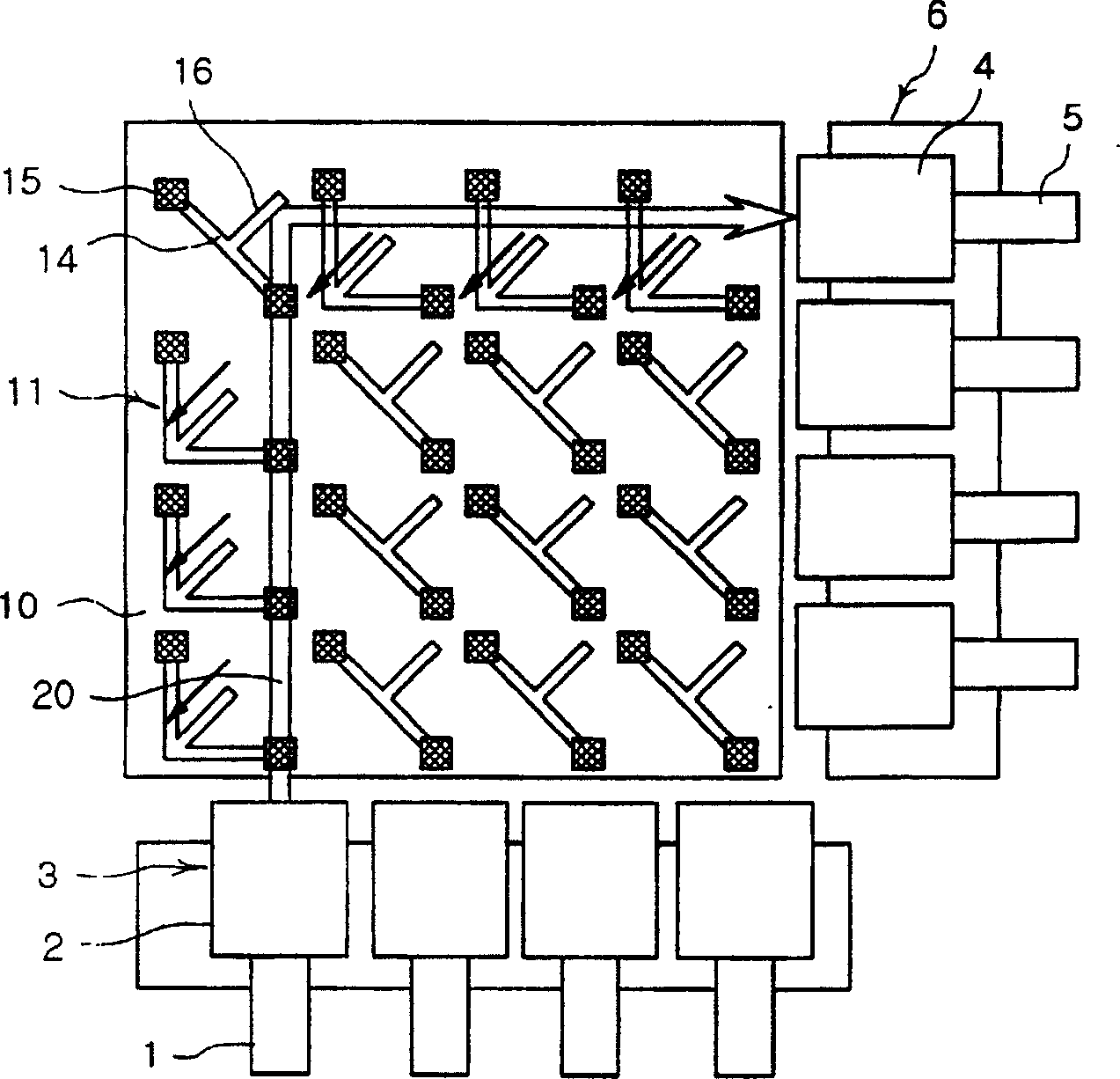
[0040] Preferred embodiments of the present invention will be described in detail below with reference to the accompanying drawings, in which image 3 is a plan view of the optical switch of the present invention, Figure 4 It is a sectional view of the optical switch of the present invention.

[0041] The optical switch of the present invention is designed such that, in the direction crossing the optical signal, the micro mirror on the optical path can be moved by the actuating element, and the actuating element is located on a layer different from the optical path, so as to improve integration.

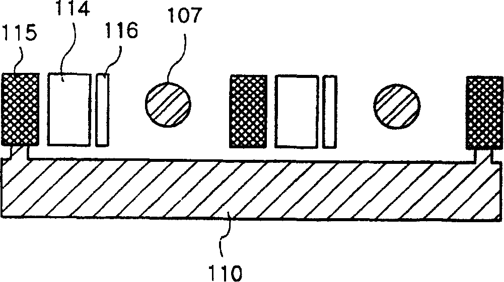
[0042] exist image 3Among them, the optical switch includes an optical signal input terminal 3 and an optical signal output terminal 6 located on the base layer. The optical signal input end 3 includes N optical fibers 1 arranged at predetermined intervals, and a lens 2 for preventing optical signal scattering is connected to the end of the optical fibers 1 . Likewise, the output ...


PUM


Abstract

The present invention relates to an optical switch and its manufacturing method. In the present invention, the base layer has an input terminal for receiving an optical signal and an output terminal for selectively receiving the optical signal from the input terminal to transmit the optical signal to the outside. In a direction crossing the optical signal, the micro-mirrors are respectively movably located on the optical signal path receiving the optical signal from the input end, so as to selectively change the optical signal from the first optical path to the second optical path. MEMS actuating elements are formed in a layer above the optical path and are connected to the micromirrors, respectively, so as to drive the micromirrors in a direction crossing the optical signal.

Description

[0001] priority [0002] This application claims the benefit of Korean Patent Application No. 2004-1360 (filing date: January 9, 2004) filed in the Korean Patent Office, the disclosure of which is incorporated herein by reference. technical field [0003] The present invention relates to an optical switch and its manufacturing method. More specifically, the optical switch and its manufacturing method of the present invention can form a dual-stage structure of micro-mirrors with different thicknesses and actuating elements, so as to facilitate manufacturing and processing. Furthermore, the optical switch and its manufacturing method in the present invention can shorten the optical path, thereby improving the integration degree and the overall optical transmission performance. Background technique [0004] As is well known in the art, a matrix optical switch (M-OSW) is a core component of optical communication technology. A matrix optical switch has a matrix consisting of N i...

Claims


Application Information

Patent Timeline
Patent Type & Authority Applications(China)
IPC IPC(8): G02B26/08B81B3/00B81B7/04B81C3/00G02B6/12G02B6/26G02B6/35G02B26/00
CPCG02B6/3514G02B6/3546G02B6/3584B81B3/0083B81C1/00142
Inventor 李贤基尹湘基
Owner SAMSUNG ELECTRO MECHANICS CO LTD
Why Eureka
Try Eureka