Manufacturing method for semiconductor integrated device
- Summary
- Abstract
- Description
- Claims
- Application Information
AI Technical Summary
Benefits of technology
Problems solved by technology
Method used
Image

Examples
Embodiment Construction
Outline of Embodiments
[0110]The following is an outline of typical embodiments of the present invention as disclosed herein.
[0111]1. A method for manufacturing a semiconductor integrated circuit device, comprising the steps of:
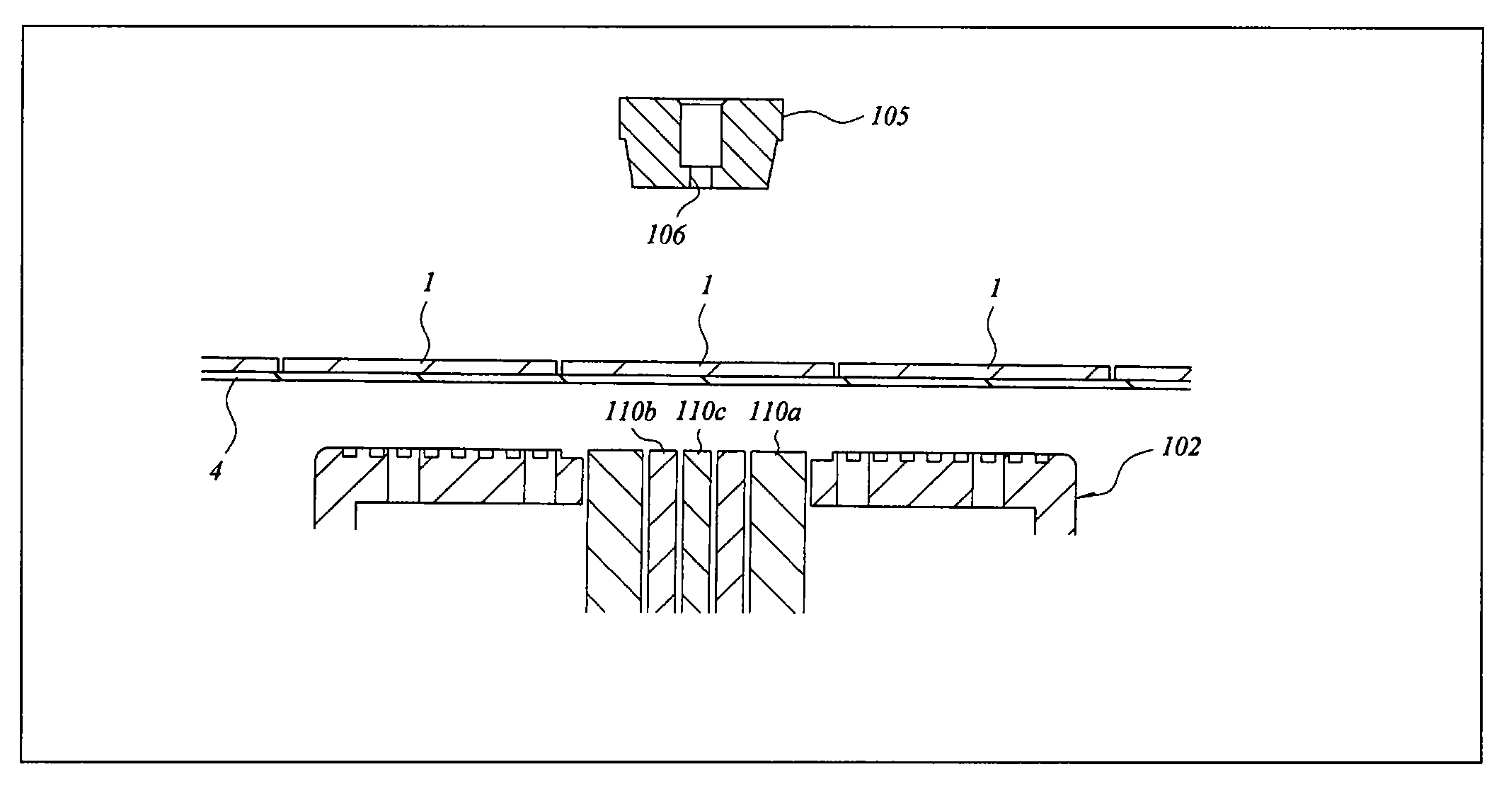
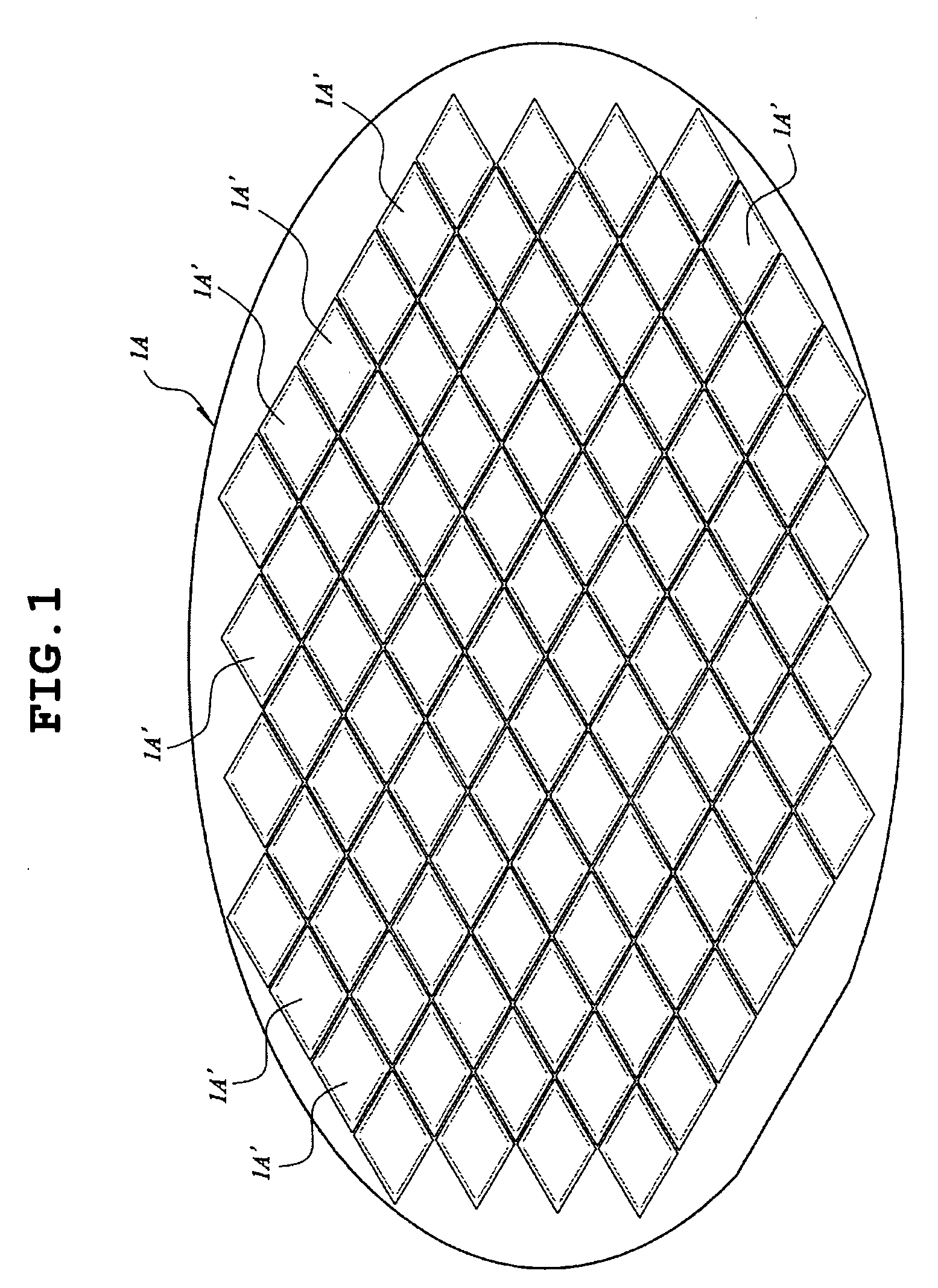
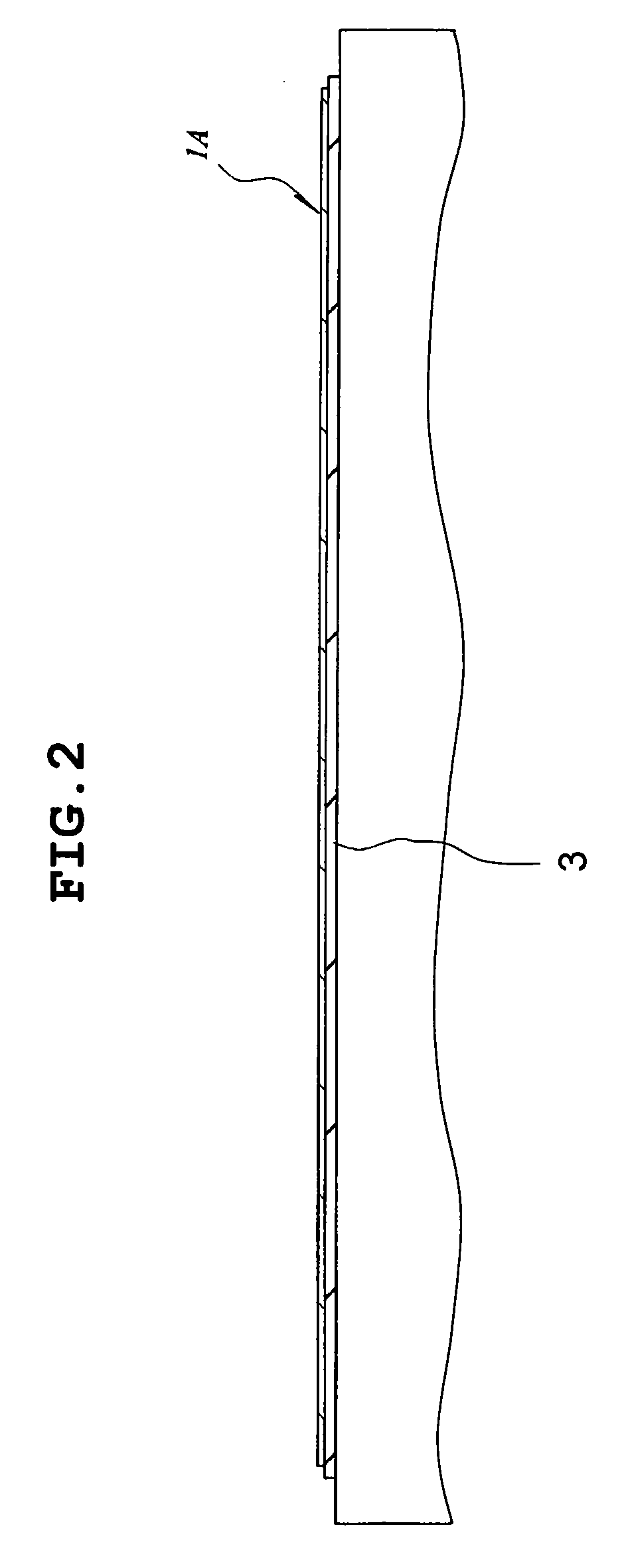
[0112](a) supplying a plurality of chips divided in individual chip regions while being arranged substantially in their original two-dimensional layout upon a wafer, to a chip treating apparatus with their back surfaces fixed to an adhesive tape; and
[0113](b) vacuum-chucking a surface of a first chip out of the chips with a chucking collet and peeling the adhesive tape from the back surface of the first chip in a state in which the adhesive tape over the back surface of the first chip is vacuum-chucked to an upper surface of a lower base,
[0114]the step (b) comprising a following sub-step of:
[0115](b1) monitoring a bent state of the first chip before complete separation of the first chip from the adhesive tape by measuring the flow rate of a vacuum chucking sys...
PUM
 Abstract
Description
Claims
Application Information
 - Generate Ideas
- Intellectual Property
- Life Sciences
- Materials
- Tech Scout
- Unparalleled Data Quality
- Higher Quality Content
- 60% Fewer Hallucinations
Browse by: Latest US Patents, China's latest patents, Technical Efficacy Thesaurus, Application Domain, Technology Topic, Popular Technical Reports.
© 2025 PatSnap. All rights reserved.Legal|Privacy policy|Modern Slavery Act Transparency Statement|Sitemap|About US| Contact US: help@patsnap.com