CMOS Compatible Microneedle Structures

a micro-needle and connector technology, applied in the field of electromechanical devices, can solve the problems of limiting the functionality of in vitro experiments on small cells, less efficient electrical coupling, and large sensors

Active Publication Date: 2008-12-25
INTERUNIVERSITAIR MICRO ELECTRONICS CENT (IMEC VZW) +1
View PDF2 Cites 43 Cited by
  • Summary
  • Abstract
  • Description
  • Claims
  • Application Information

AI Technical Summary

Benefits of technology

[0018]An advantage of this method is the fact that CMOS processing allows the combination with CMOS devices in the substrate and devices for sensing and/or actuation purposes on top of the microneedles. CMOS processing also allows one to make small-size needles making it possible to contact small cells, such as neurons.

Problems solved by technology

These sensors are often relatively big and only small matrices or arrays of micro-electrodes can be made.
In the case of mammalian neurons, e.g., hippocampal neurons, the cells are much smaller, which leads to a less efficient electrical coupling.
Various micro

Method used


Image

  • CMOS Compatible Microneedle Structures
  • CMOS Compatible Microneedle Structures
  • CMOS Compatible Microneedle Structures

Examples


example 1

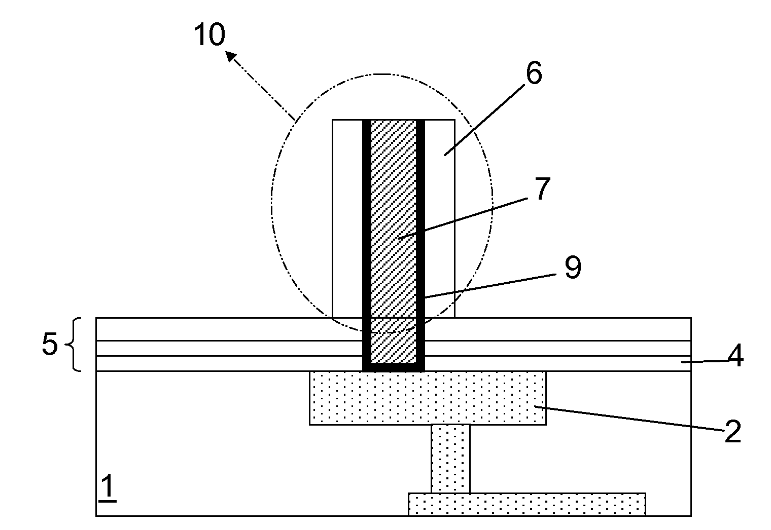
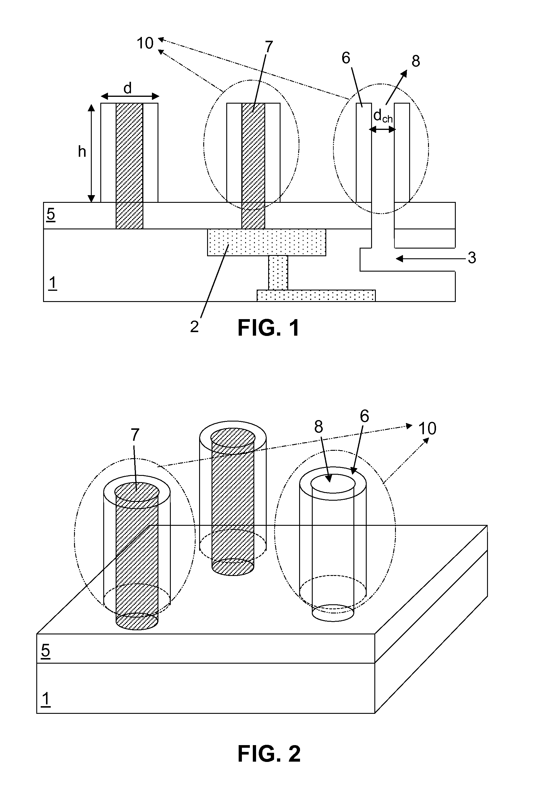
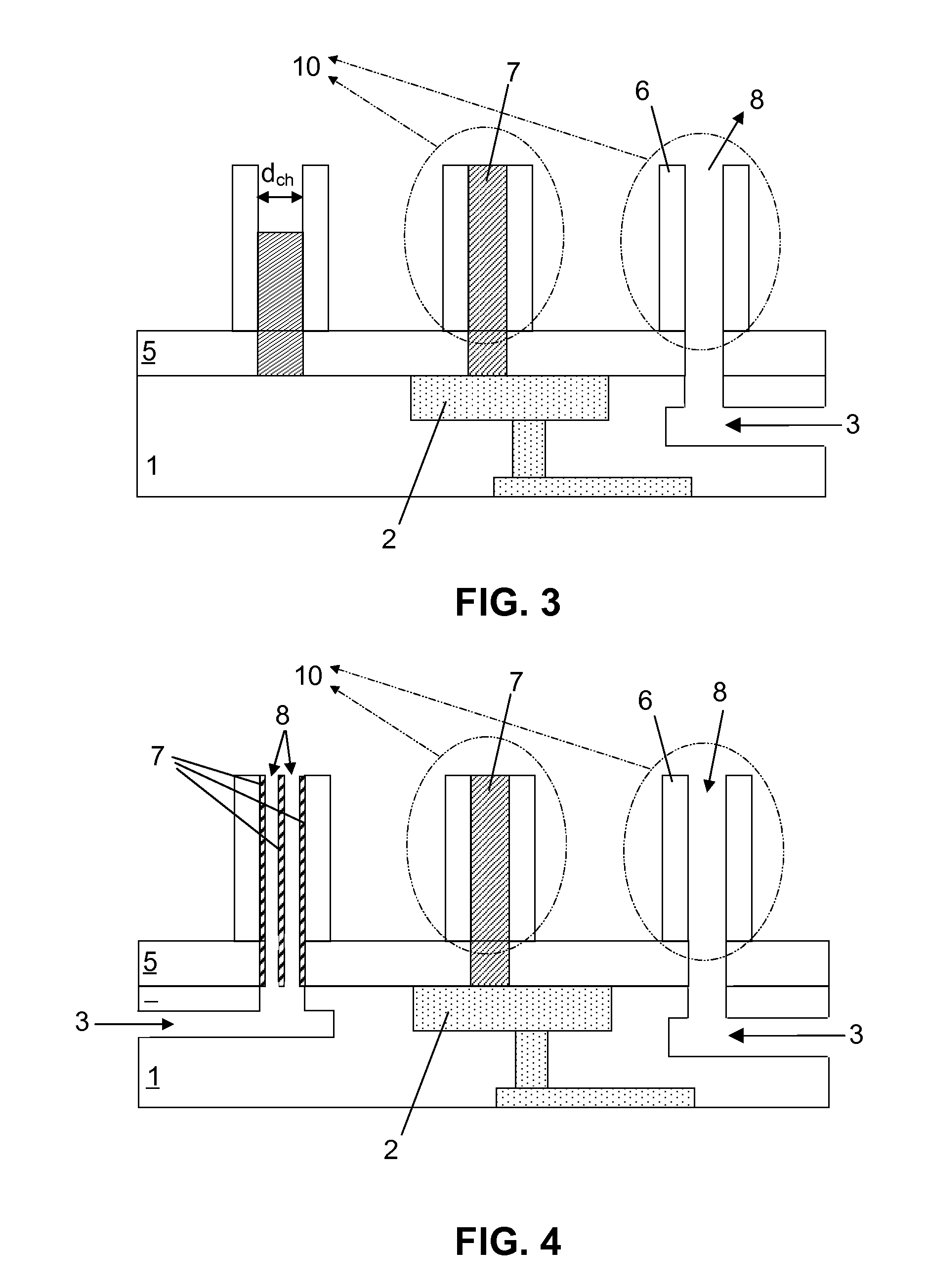
[0140]Microneedles 10 with a width of approximately 250 nm and a height of 1 μm were produced using a Cu damascene approach. The microneedles 10 were further oxidized or electroplated with a noble metal to prevent Cu-induced cytotoxicity.

[0141]Cu microneedles 10 comprising a SiO2 isolation layer 6 have been made using CMOS processing techniques. The different processing steps are described below. The steps refer to the steps as presented in FIG. 11.

[0142]First (see FIG. 11(a)) 8″ Si wafers 31 with a Cu damascene metal pattern 32 in a SiO2 dielectric 33 were created. The pads in this Cu damascene metal layer 32 are acting as base on which the microneedles 10 will be formed. On top a layer 34 of 50 nm SiC was deposited. The SiC layer 34 will act as a diffusion barrier between the Cu and the underlying electronic circuitry 32 (Cu diffusing in the liquid is toxic for the cells) and is also used as an etch stop layer.

[0143]Subsequently, a layer 35 of oxide was deposited (see FIG. 11(b))....


PUM


Abstract

The present invention provides an electronic device for sensing and/or actuating, the electronic device comprising at least one microneedle (10) on a substrate (1), each of the microneedles (10) comprising at least one channel (7, 8) surrounded by an insulating layer (6). The present invention also provides a method for making such an electronic device for sensing and/or actuating.

Description

CROSS-REFERENCE TO RELATED APPLICATIONS[0001]The present application claims priority under 35 U.S.C. § 119(e) to U.S. Provisional Patent Application No. 60 / 893,699, filed Mar. 8, 2007, the entirety of which is incorporated herein by reference.FIELD OF THE INVENTION[0002]The invention relates to electronic devices for sensing and / or actuating comprising at least one microneedle, and to a method for making such electronic devices.BACKGROUND OF THE INVENTION[0003]Sensors comprising micro-electrode arrays are used for measuring electrical activity in small networks of neurons. These sensors are often relatively big and only small matrices or arrays of micro-electrodes can be made. Current state-of-the art micro-electrode arrays (MEAs) may contain a maximum of 64 electrodes with a minimal spacing of 100 μm between neighbouring electrodes. The electrodes are often made of flat TiN pads with a maximum diameter of 10 μm. For some applications, smaller spacings, e.g., <10 μm, and a larger...

Claims


Application Information

Patent Timeline
IPC IPC(8): A61B5/055H01L21/283
CPCG01N33/48728Y04S10/54G06N3/061A61M37/0015A61M2037/0053
Inventor HUYS, ROELANDBARTIC, CARMENLOO, JOSINE
Owner INTERUNIVERSITAIR MICRO ELECTRONICS CENT (IMEC VZW)
Why Eureka
Try Eureka