Level shifter having low duty cycle distortion

a level shifter and duty cycle distortion technology, applied in logic circuits, pulse automatic control, pulse techniques, etc., can solve the problem of introducing an undesirable amount of duty cycle distortion into the signal, the duty cycle distortion of the circuit of fig. 1 can be greater than, and the low-to-high and high-to-low propagation delay times differ from one another, so as to achieve the effect of low duty cycle distortion and increase the supply voltage margin of the level shifter circui

Active Publication Date: 2009-01-01
QUALCOMM INC
View PDF12 Cites 20 Cited by
  • Summary
  • Abstract
  • Description
  • Claims
  • Application Information

AI Technical Summary

Benefits of technology

[0014]The propagation delay through the level shifter circuit for a low-to-high transition of the input signal IN differs from the propagation delay through the level shifter circuit for a high-to-low transition of the input signal IN by an amount of time referred to here as the “duty cycle distortion skew”. In one example, the duty cycle distortion skew is less than 50 picoseconds over operating voltage, process and operating temperature corners, when the level shifter circuit has a supply voltage margin of more than one quarter of a nominal 1.2 volt value of the first supply voltage VDDL. Due to the architecture of the level shifter circuit, the low duty cycle distortion skew is achieved without having to balance operating characteristics of the P-channel and an N-channel transistors within the cross-coupled level shifting latch. Because P-channel and N-channel transistors within the cross-coupled level shifting latch do not have to be balanced, the size of the N-channel transistors can be increased relative to the P-channel transistors, thereby increasing the supply voltage margin of the level shifter circuit.

Problems solved by technology

The level shifting circuit of FIG. 1 works well in many applications, but as signal speeds increase, the level shifting circuit is seen to introduce an undesirable amount of duty cycle distortion skew into the signal.
Unfortunately, as the operating voltages, process and temperature of the circuit vary, the low-to-high and high-to-low propagation delay times differ from one another.
Unfortunately, the circuit of FIG. 1 can have a duty cycle distortion greater than this.

Method used


Image

  • Level shifter having low duty cycle distortion
  • Level shifter having low duty cycle distortion
  • Level shifter having low duty cycle distortion

Examples


Embodiment Construction

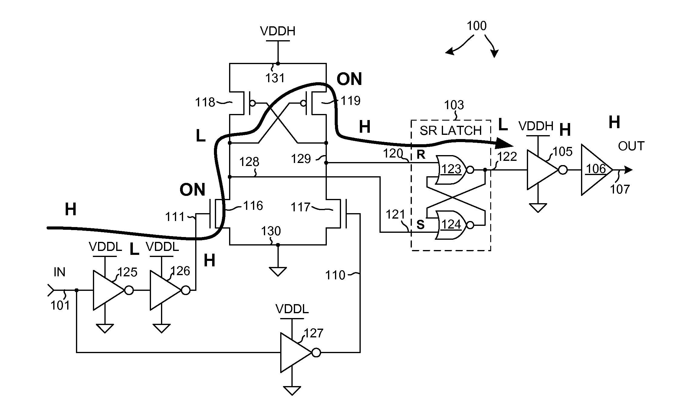
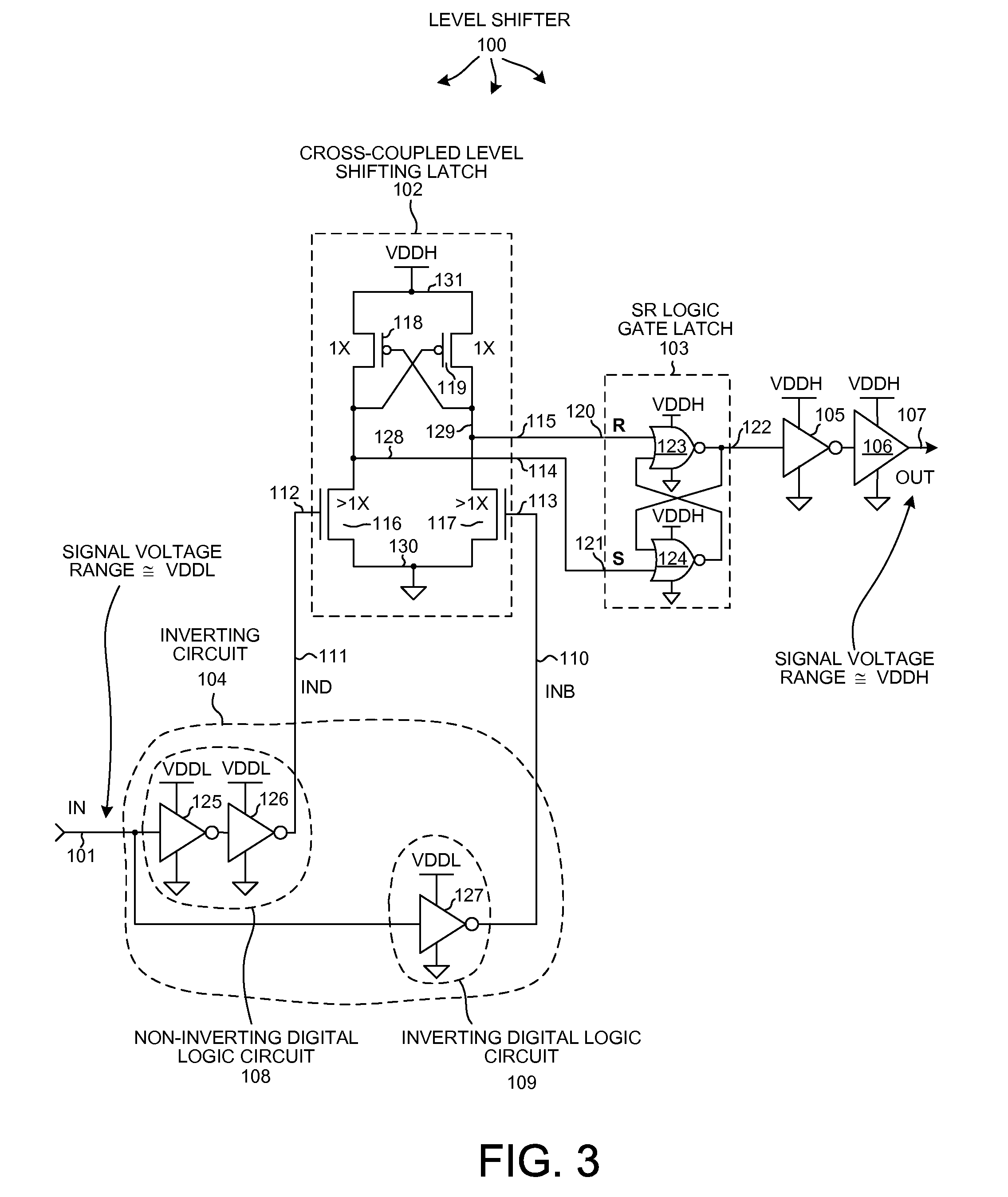
[0024]FIG. 3 is a simplified diagram of a level shifting circuit 100 in accordance with one novel aspect. Level shifting circuit 100 includes an input node 101, a cross-coupled level shifting latch 102, a set-reset (SR) logic gate latch 103, an inverting circuit 104, an inverter 105, a buffer 106, and an output node 107. A digital input signal IN is received onto input node 101 and is level shifted and output as a digital output signal OUT onto output node 107. Digital input signal IN transitions within a first signal voltage range (for example, from ground potential to a VDDL voltage of approximately 1.2 volts). Digital output signal OUT transitions within a second signal voltage range (for example, from the ground potential to a VDDH voltage of approximately 1.8 volts). Level shifting circuit 100 is realized in complementary logic involving P-channel and N-channel field effect transistors.

[0025]Inverting circuit 104 includes a non-inverting digital logic circuit 108 and an inverti...


PUM


Abstract

A level shifter includes an inverting circuit, a cross-coupled level shifting latch, and a SR logic gate latch. The first and second outputs of the level shifting latch are coupled to the set (S) and reset (R) inputs of the SR latch. The inverting circuit, that is powered by a first supply voltage VDDL, supplies a noninverted version of an input signal onto a first input of the level shifting latch and supplies an inverted version of the input signal onto a second input of the level shifting latch. A low-to-high transition of the input signal resets the SR latch, whereas a high-to-low transition sets the SR latch. Duty cycle distortion skew of the level shifter is less than fifty picoseconds over voltage, process and temperature corners, and the level shifter has a supply voltage margin of more than one quarter of a nominal value of VDDL.

Description

BACKGROUND INFORMATION[0001]1. Technical Field[0002]The disclosed embodiments relate to level shifting circuits, and more particularly relate to high speed level shifting circuits that exhibit both low duty cycle distortion and high supply voltage margin.[0003]2. Background Information[0004]Digital logic circuits can be powered from different supply voltages. In one example, an integrated circuit includes a first digital logic block that operates with a first supply voltage as well as a second digital logic block that operates with a second supply voltage. If a digital signal is to pass form one logic block to the other, the digital levels of the signal must be shifted. A circuit referred to as a level shifter is sometimes used to perform this level shifting function.[0005]FIG. 1 (Prior Art) is a circuit diagram of a conventional level shifter 1. The label VDDL designates a first supply voltage (for example, 1.2 volts) whereas the label VDDH designates a second supply voltage (for e...

Claims


Application Information

Patent Timeline
Patent Type & Authority Applications(United States)
IPC IPC(8): H03K19/0175
CPCH03K3/356113
Inventor LEE, CHULKYU
Owner QUALCOMM INC
Why Eureka
Try Eureka