Apertured chip resistor and method for fabricating same

a technology of apertured chip and resistor, which is applied in the manufacture of resistor chips, resistor details, resistor manufacturing, etc., can solve the problems of high-frequency signal degradation, low cost of resistor mass production, and difficult control of resistance film thickness uniformity, so as to reduce the total production cost, reduce the drawback of high application cost, and increase the yield of fabrication process

Inactive Publication Date: 2009-01-01
FEEL CHERNG ENTERPRISE
View PDF0 Cites 5 Cited by
  • Summary
  • Abstract
  • Description
  • Claims
  • Application Information

AI Technical Summary

Benefits of technology

[0019]In view of the aforementioned descriptions, the apertured fixed chip resistor and method for fabricating the same of the present invention has the following main features: by applying a bonding layer to bond the substrate and the metallic sheet structure together, the present invention is capable of eliminating the drawback of the high cost of applying semiconductor fabrication processing and consequently achieving the objectives of a simple fabrication process, increasing fabrication process yield, and decreasing total production costs. The surface of the part of the metallic sheet structure not covered by the passivation layer is divided to directly form two electrode zones, which provide a means for either a direct soldering application or for further forming electrodes that are advantageous for soldering, thereby eliminating unnecessary current transmission impedance as in the prior art, as well as effectively and stably reducing the temperature coefficient of resistance.

Problems solved by technology

However, printing and coating techniques, which are presently the most applied fabrication techniques of the prior arts, have practical disadvantages that hinder mass production at low cost.
However, the resistant film is formed by means of printing technique, and it is difficult to control the uniformity of thickness of the resistant film.
This is especially significant when the aforementioned chip resistor is applied in a high frequency environment, because the resistant film has high porosity and a loose structure and consequently causes high-frequency signals to degrade greatly.
Therefore it is not applicable to or ideal for high-frequency products.
However, since these methods of fabricating chip resistors involve semiconductor fabrication processing, the required equipment investment is high, and also the semiconductor process yield has its limitations, making the overall production cost quite high, thereby greatly decreasing the competitive advantage of such products.
However, in the process of removing the photoresist film, the situation of incomplete removal or excessive removal often happens.
Consequently, the resistant film is easily exposed, and it can then get contaminated or become oxidized, thereby affecting its electrical properties, and accordingly decreasing the fabrication process yield.
Consequently, the problems of high cost and poor yield are still unsolved; and the coating process for the passivation layer raises the cost even more.
In addition, the resistant film is indirectly electrically connected to the plane electrodes via the main electrodes, thereby increasing the temperature coefficient of resistance of the resistance film and the main electrodes, and consequently the temperature coefficient of resistance of the fabricated chip resistor can not be reduced to the demanded value, and also the heat dissipation efficiency is significantly decreased.
In summary, the aforementioned prior art has the drawbacks of a low fabrication process yield, unavoidably high equipment and production costs, incapability of reducing the temperature coefficient of resistance to demanded values, and others.

Method used


Image

  • Apertured chip resistor and method for fabricating same
  • Apertured chip resistor and method for fabricating same
  • Apertured chip resistor and method for fabricating same

Examples


Embodiment Construction

[0024]The following illustrative embodiments are provided to illustrate the disclosure of the present invention; these and other advantages and effects can be readily understood by those in the art after reading the disclosure of this specification. The present invention can also be performed or applied by other differing embodiments. The details of the specification may be changed on the basis of different points and applications, and numerous modifications and variations can be devised without departing from the spirit of the present invention.

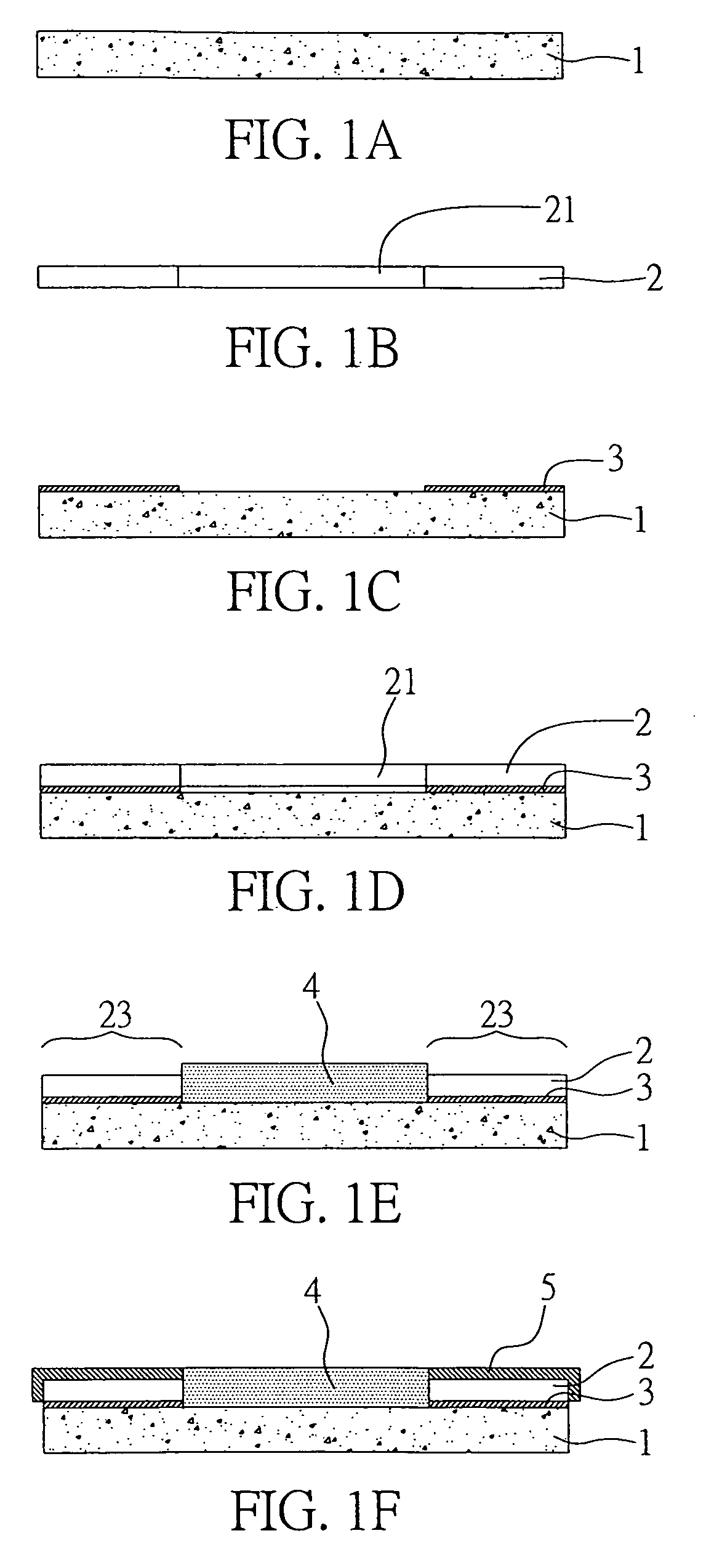
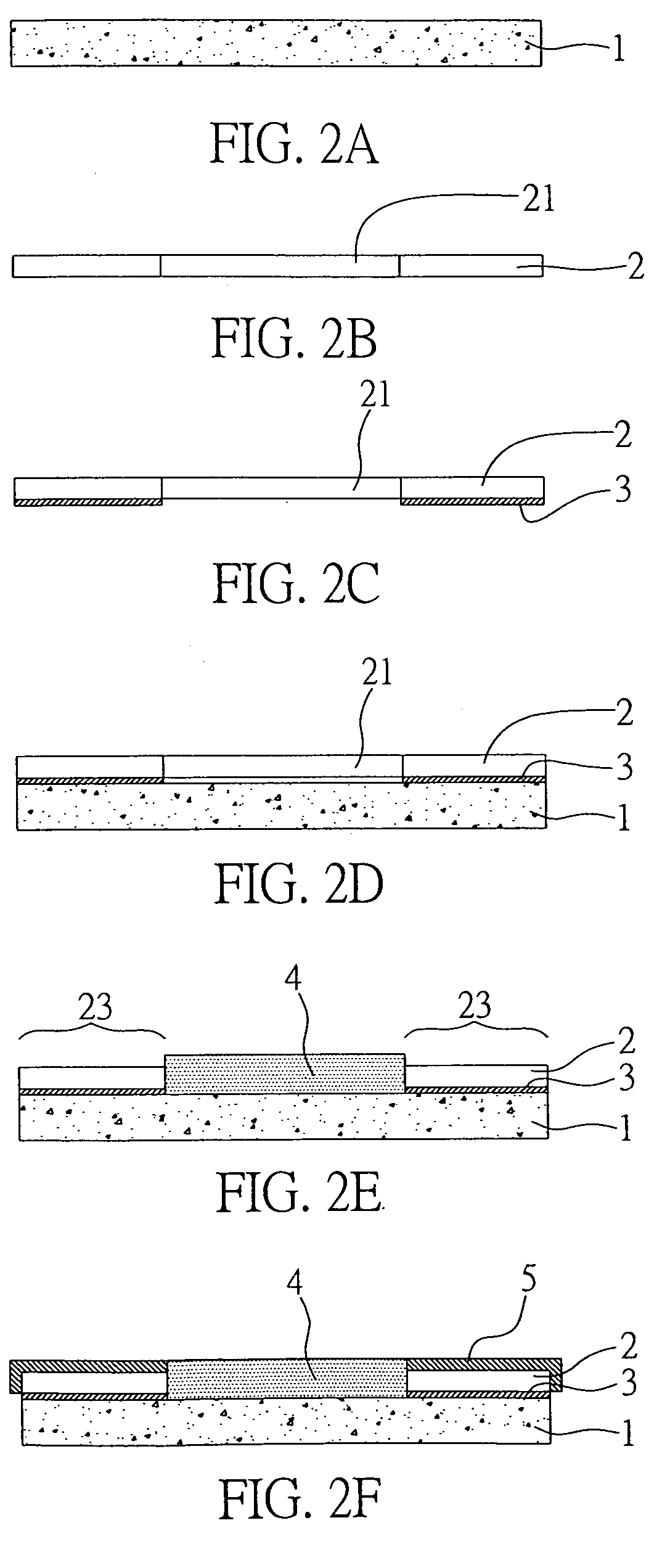
[0025]FIGS. 1A through 1G are flow chart diagrams of the first embodiment of fabrication method of apertured fixed chip resistor according to the present invention. As shown in the figures, the fabrication method for an apertured fixed chip resistor provided by the present invention comprises but is not restricted to the following descriptions.

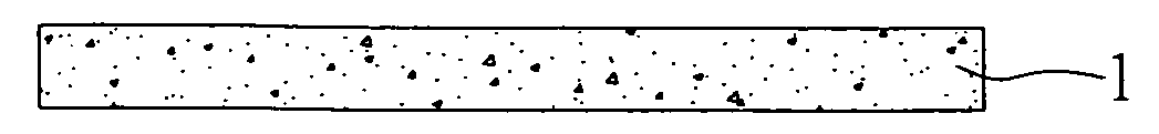
[0026]As shown in FIGS. 1A and 1B, first a substrate 1 and a metallic sheet structure 2 that has a ...


PUM

PropertyMeasurementUnit
resistancesaaaaaaaaaa
resistanceaaaaaaaaaa
shapeaaaaaaaaaa

Abstract

An apertured fixed chip resistor and method for fabricating the same are disclosed according to the present invention, wherein a bonding layer is applied to accordingly bond together a substrate and a metallic sheet structure that has central aperture, and then a passivation layer is applied to partially cover the exposed surface of the metallic sheet structure and to divide the surface of the metallic sheet structure into a central covered region separating two uncovered regions, wherein the uncovered regions are provided to serve as electrode zones, thereby eliminating unnecessary current transmission impedance as in prior art as well as efficiently and stably reducing the temperature coefficient of resistance. The bonding design of the substrate and the metallic sheet structure of the present invention is capable of overcoming the drawback of the high cost of semiconductor processing as applied in prior art, and it provides a simple fabrication process that is capable of increasing process yield and decreasing total production costs.

Description

BACKGROUND OF THE INVENTION[0001]1. Field of the Invention[0002]This invention generally relates to chip resistors, and more specifically, to an apertured chip resistor and a method for fabricating the same.[0003]2. Description of Related Art[0004]In accordance with the trend towards microminiaturization and portability of various electronic devices, fixed chip resistors—which are frequently applied in circuits for measuring the electric potential difference between two terminals—are accordingly trending towards microminiaturization as well. But in order to reduce measurement errors as well as raise detected current values, and to reduce the temperature coefficient of resistance, resistors with resistances ranging from 0.02Ω to 10Ω that are capable of handling high power with wattage ratings often over 0.1 W are commonly demanded. However, printing and coating techniques, which are presently the most applied fabrication techniques of the prior arts, have practical disadvantages that...

Claims


Application Information

Patent Timeline
Patent Type & Authority Applications(United States)
IPC IPC(8): H01C1/012H01C17/00
CPCH01C1/012H01C1/142Y10T29/49082H01C17/006H01C7/003
Inventor TSAI, RONG-TZER
Owner FEEL CHERNG ENTERPRISE
Why Eureka
Try Eureka