Dielectric ceramic composition, ceramic substrate, and method for producing the same
- Summary
- Abstract
- Description
- Claims
- Application Information
AI Technical Summary
Benefits of technology
Problems solved by technology
Method used
Image


Examples
Embodiment Construction
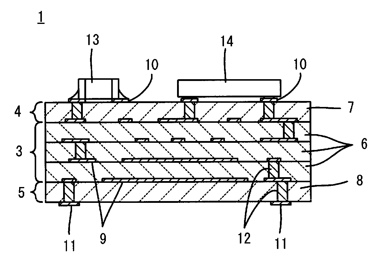
[0032]FIG. 1 is a sectional view of a multilayer ceramic substrate 1 according to a preferred embodiment of the present invention.
[0033]The multilayer ceramic substrate 1 has a laminated structure including an inner layer portion 3 and first and second outer layer portions 4 and 5 arranged with the inner layer portion 3 disposed therebetween in the lamination direction. The inner layer portion 3 includes at least one inner layer-portion ceramic layer 6. The first outer layer portion 4 includes at least one outer layer-portion ceramic layer 7. The second outer layer portion 5 includes at least one outer layer-portion ceramic layer 8.
[0034]The multilayer ceramic substrate 1 includes a conductor pattern that preferably primarily includes silver or copper, for example. The conductor pattern is used, for example, to define passive devices, such as capacitors and inductors, or to provide connection wiring such as electrical connections between devices, for example. The conductor pattern t...
PUM
| Property | Measurement | Unit |
|---|---|---|
| Fraction | aaaaa | aaaaa |
| Fraction | aaaaa | aaaaa |
| Fraction | aaaaa | aaaaa |
Abstract
Description
Claims
Application Information