Semiconductor device

a technology of semiconductors and devices, applied in the direction of semiconductor devices, basic electric elements, electrical appliances, etc., can solve the problems of high gate leak current density and limited operation drain voltage, and achieve the effect of reducing gate leak curren

Inactive Publication Date: 2009-01-08
NEC CORP
View PDF5 Cites 13 Cited by
  • Summary
  • Abstract
  • Description
  • Claims
  • Application Information

AI Technical Summary

Benefits of technology

[0010]According to a semiconductor device of this configuration, an Al composition ratio x1 (x1>0) at an interface with a channel layer of an electron supply layer and an Al composition ratio xa (xa>0) at an interface with a gate electrode of an electron supply layer are x1 / 2≦xa<x1 and x1≦0.3; and therefore, there may be provided a semiconductor device which may reduce a gate leak current.
[0011]According to the present invention, there is provided a semiconductor device which may reduce a gate leak current.

Problems solved by technology

Therefore, there is a problem in that the III group nitride based HJFET using AlGaN as the electron supply layer has high gate leak current density and operation drain voltage is limited.

Method used


Image

  • Semiconductor device
  • Semiconductor device
  • Semiconductor device

Examples


Embodiment Construction

[0034]First, in order to facilitate understanding of the present invention, a general outline of the present invention will be described.

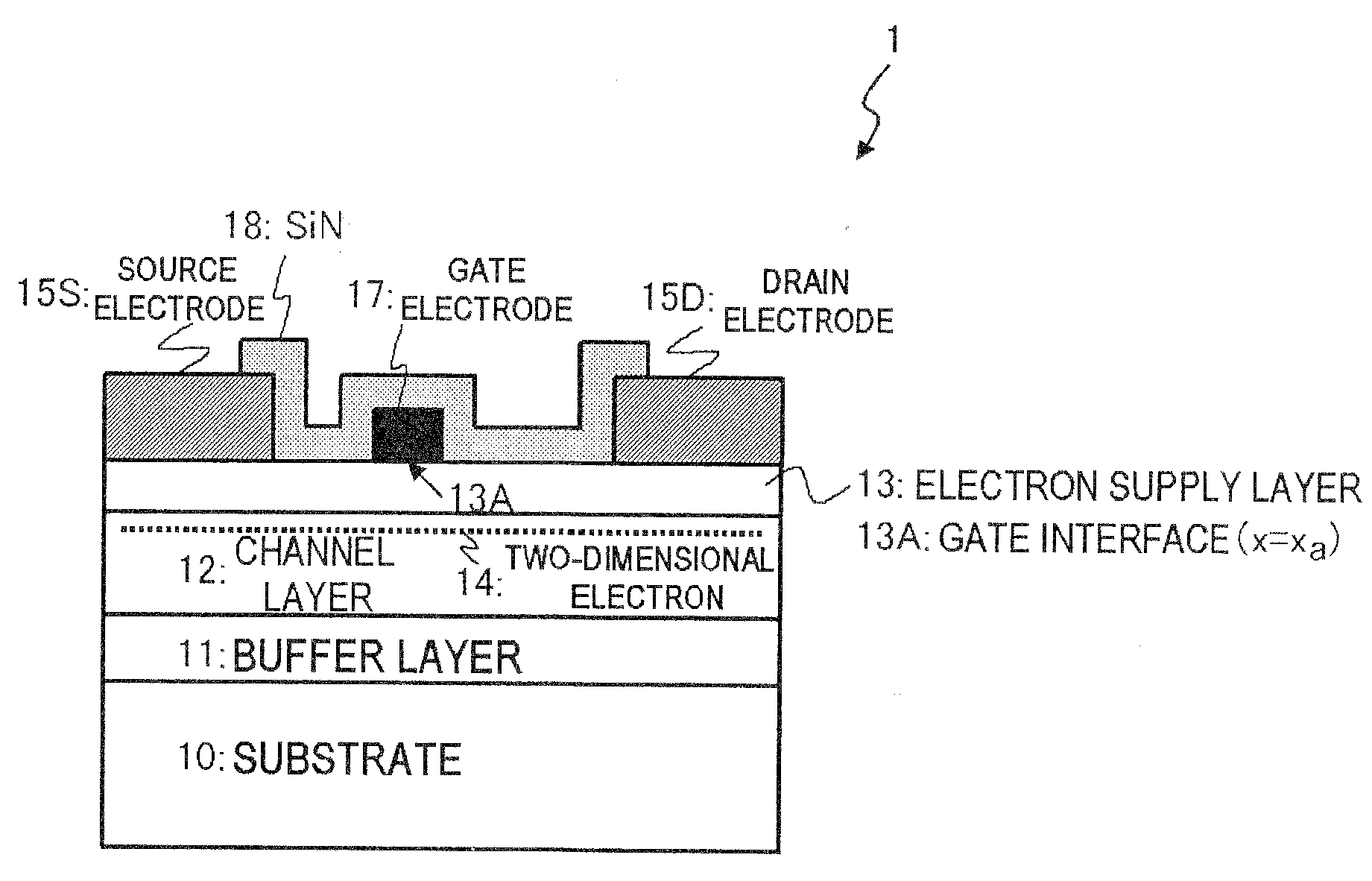
[0035]FIG. 1 shows an HJFET (semiconductor device) 1 as one example of a semiconductor device according to the present invention.

[0036]The HJFET 1 has a silicon carbide (SiC) substrate 10; a buffer layer 11 made of an aluminum nitride (AlN) layer which is stacked on the silicon carbide (SiC) substrate 10, a channel layer 12 made of InyGa1-yN (0≦y≦1) (in this case, made of undoped GaN) which is stacked on the buffer layer 11; an electron supply layer 13 stacked on the channel layer 12; and a gate electrode 17, a source electrode 15S, and a drain electrode 15D, those of which are formed in contact with the electron supply layer 13 on the electron supply layer 13.

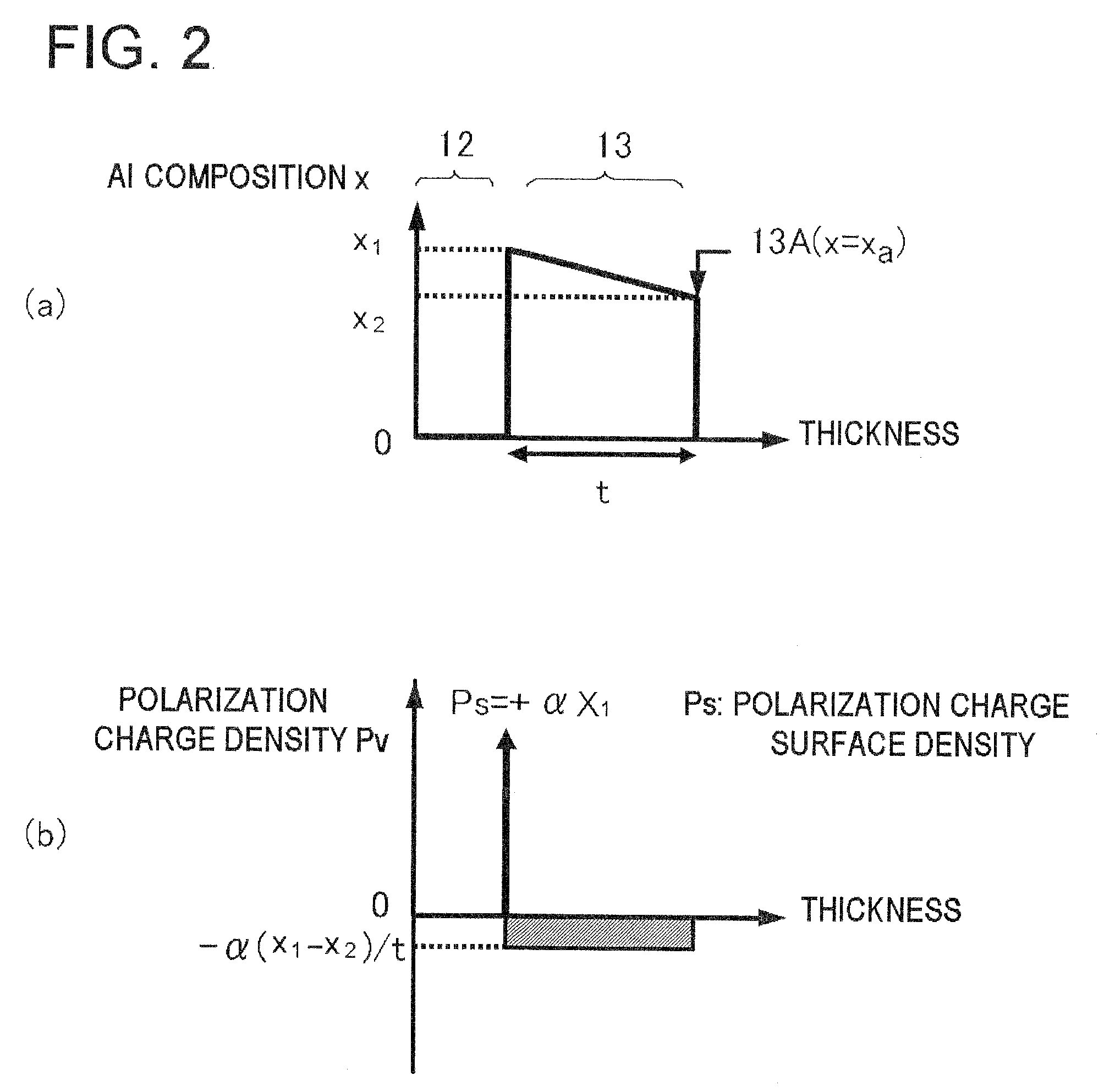
[0037]The electron supply layer 13 is a layer which forms a heterojunction with the channel layer 12 and contains InzAlxGa1-z-xN (0≦z13 is an undoped AlxGa1-xN (012 side toward the gate elect...


PUM


Abstract

An electron supply layer (13) is a layer which forms a heterojunction with a channel layer (12) and contains InzAlxGa1-zxN (0≦z<1, 0<x<1, 0<x+z<1). On the electron supply layer (13), a gate electrode (17) is formed in contact with the electron supply layer (13). The Al composition ratio x1 at the interface between the electron supply layer (13) and the channel layer (12) and the Al composition ratio xa at the interface between the electron supply layer (13) and the gate electrode (17) satisfy the following conditions:x1 / 2≦xa<x1 andx1≦0.3.

Description

TECHNICAL FIELD[0001]The present invention relates to semiconductor devices and, more particularly, relates to a heterojunction field effect transistor (HJFET) which contains a III group nitride semiconductor as a material.BACKGROUND ART[0002]FIG. 20 is a view showing a cross sectional structure of an HJFET according to a related art. Such an HJFET is reported in a non-patent document 1, for example.[0003]In FIG. 20, reference numeral 200 denotes a substrate, 201 denotes a buffer layer, 202 denotes a gallium nitride (GaN) channel layer, and 203 denotes an aluminum gallium nitride (AlbGa1-bN (b is constant) electron supply layer. With piezo polarization effects and spontaneous polarization effects, both being caused by a lattice constant difference between GaN and AlGaN, a two-dimensional electron gas 204 is formed in the vicinity of an interface between the GaN channel layer 202 and the AlGaN electron supply layer 203. A source electrode 205S and a drain electrode 205D are formed in...

Claims


Application Information

Patent Timeline
Patent Type & Authority Applications(United States)
IPC IPC(8): H01L29/778
CPCH01L29/2003H01L29/7787H01L29/201
Inventor ANDO, YUJIMIYAMOTO, HIRONOBUOKAMOTO, YASUHIRONAKAYAMA, TATSUOINOUE, TAKASHI
Owner NEC CORP
Why Eureka
Try Eureka