Photo detector, image sensor, photo-detection method, and imaging method

a technology of image sensor and detector, which is applied in the field of photo detector, image sensor, photodetection method, imaging method, can solve the problems of loss of light caused by color filter, difficulty in reducing cost, so as to achieve satisfactory color separability, reduce device thickness, and suppress color mixing

Inactive Publication Date: 2009-01-08
CANON KK
View PDF8 Cites 78 Cited by
  • Summary
  • Abstract
  • Description
  • Claims
  • Application Information

AI Technical Summary

Benefits of technology

[0013]The present invention provides a photo detector, an image sensor, a photo-detection method, and an imaging method in which the thickness of the device can be reduced, color mixing can be suppressed, satisfactory color separability can be achieved together with high sensitivity, chemical stability can be achieved, and the compatibility of a production process of the device with a production process of peripheral circuits can be realized.
[0023]Various aspects of the present invention can provide a photo detector that can adjust the spectral sensitivity without using a color filter. For example, a device according to an aspect of the present invention can have a reduced thickness. Accordingly, color mixing can be suppressed, and satisfactory color separability can be achieved together with high sensitivity. Furthermore, various aspects of the present invention can provide a photo detector and an image sensor that have excellent chemical stability and in which compatibility of a production process of the device with a production process of peripheral circuits can be achieved. Furthermore, a photo-detection method and an imaging method using such a device can be realized.

Problems solved by technology

Accordingly, forming different color filters for small areas makes it difficult to decrease the cost.
However, image sensors utilizing an arrangement of color filters has some problems.
One of the problems is the loss of light caused by using color filters.
Another problem is the decrease in the resolution caused by a low-pass filter.
As a result, the image sensor may not be sensitive particularly to red (R) light for which the absorption coefficient of Si is low.
In the photo detector disclosed in Japanese Patent Laid-Open No. 2007-13065, since the periodic structure is composed of SiO2 having a low loss, a resonance peak becomes steep, and this structure is not necessarily suitable for color separation of visible light.
Therefore, this device is disadvantageous in that the film thickness of the device is large, and color mixing easily occurs when light is incident at an angle (see a description below of the case where a thick photo detector 902 is used, as shown in FIG. 9B).
Furthermore, this device is disadvantageous in that it is difficult to achieve satisfactory color separability together with a high sensitivity.
However, this sensor has a problem of chemical instability, because an organic substance is used.
In addition, this sensor is disadvantageous in that the sensitivity is not satisfactory because of its low carrier mobility.
Furthermore, this sensor also has a problem in terms of the incompatibility of a production process of the sensor with a production process of peripheral circuits, such as a readout circuit and an amplifying circuit.

Method used


Image

  • Photo detector, image sensor, photo-detection method, and imaging method
  • Photo detector, image sensor, photo-detection method, and imaging method
  • Photo detector, image sensor, photo-detection method, and imaging method

Examples


first embodiment

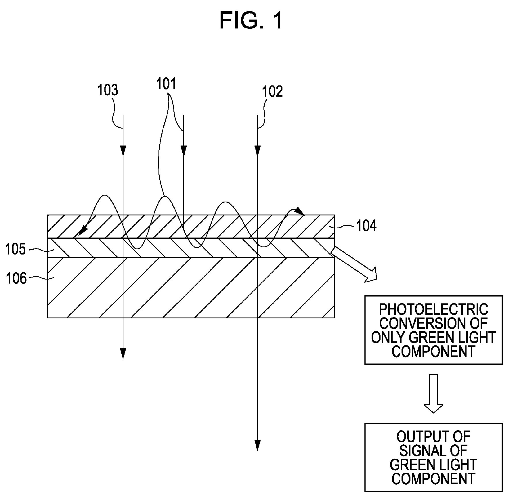
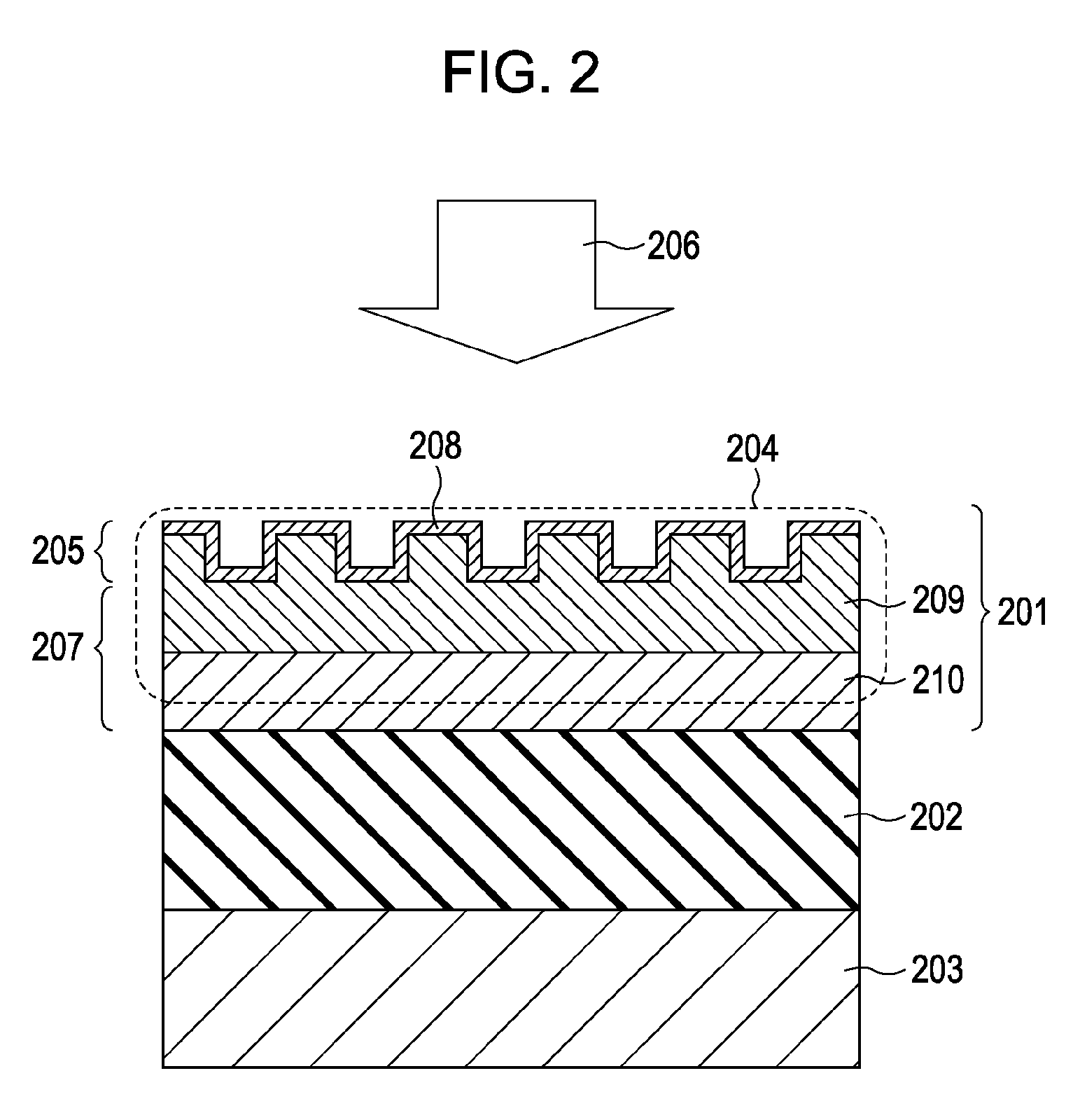
[0094]FIG. 2 shows an example of a photo detector according to the first aspect of the present invention. A photoelectric conversion (layer) area 204 is provided in a silicon-on-insulator (SOI) substrate composed of a Si layer 201, a SiO2 layer 202, and a Si substrate layer 203. A periodic structure 205 composed of two-dimensional irregularities is formed on the top surface of the photoelectric conversion region 204. Depressions of the periodic structure may reach the insulating layer of the SOI substrate or may not reach the insulating layer. A protective film may be optionally provided on the top surface.

[0095]When incident light 206 is incident on the photo detector of this embodiment, the light is diffracted by the two-dimensional periodic structure 205 provided on the surface of the photo detector. A light component in a specified wavelength range, depending on parameters of the periodic structure 205, generates guided-mode resonance. Guided-mode resonance is a phenomenon in wh...

second embodiment

[0103]FIG. 4 shows another embodiment of the photo detector of the present invention. In the photo detector shown in FIG. 4, a photoelectric conversion region 404 is provided in a silicon-on-insulator (SOI) substrate composed of a Si layer 401, a SiO2 layer 402, and a Si substrate layer 403. An insulating film (protective film) 405 made of SiO2 is provided on the top surface of the photoelectric conversion material. Furthermore, a two-dimensional periodic structure 407 made of amorphous Si 406 is formed on the insulating film 405. When incident light 408 is incident on the photo detector of this embodiment, the light is diffracted by the two-dimensional periodic structure 407 provided on the surface of the photo detector. A light component in a specified wavelength range, depending on parameters of the periodic structure 407, generates guided-mode resonance. Guided-mode resonance is a phenomenon in which light diffracted by a periodic structure is coupled with guided light, thereby ...

third embodiment

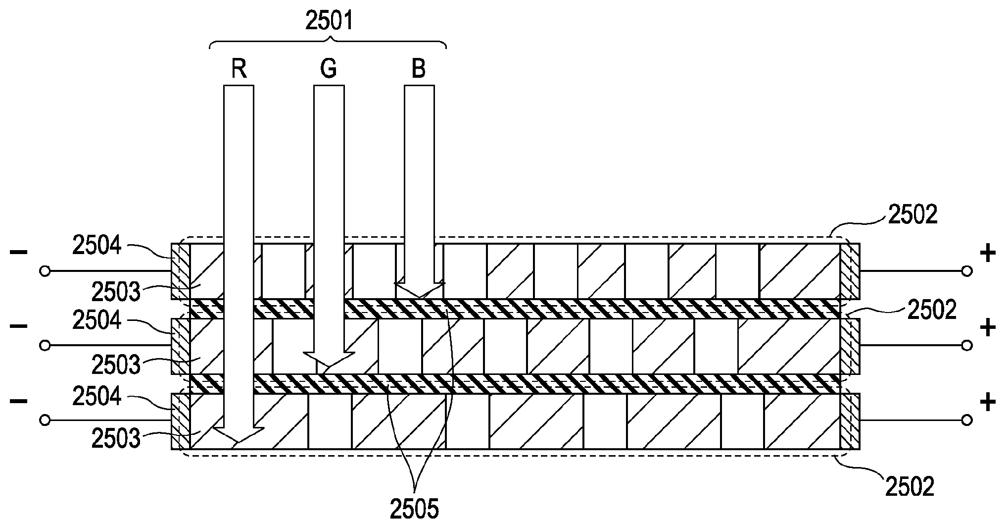
[0109]An embodiment of an image sensor according to the first aspect of the present invention is shown in FIGS. 6A and 6B. FIG. 6A is a plan view of a light-receiving surface constituting a surface on which light is incident. FIG. 6B is a cross-sectional view taken along broken line VIB-VIB in FIG. 6A. In the device shown in FIGS. 6A and 6B, a plurality of photo detectors 601 for performing a two-dimensional imaging are arranged. An irregular periodic structure is formed on the surface of each of the photo detectors 601. An area 602 that resonates with a red (R) light component, an area 603 that resonates with a green (G) light component, and an area 604 that resonates with a blue (B) light component are provided. For example, by forming periodic structures on the basis of the parameters described in the first embodiment, peak wavelengths can be provided at 450 nm, 550 nm, and 650 nm.

[0110]As described in the first embodiment, regarding incident light 605 diffracted by the irregular...


PUM


Abstract

A photo detector includes a photoelectric conversion layer having a periodic structure made of a semiconductor material on a surface of the photoelectric conversion layer. In the photo detector, at least a part of a resonance region formed by the periodic structure is included in the photoelectric conversion layer of the photo detector.

Description

BACKGROUND OF THE INVENTION[0001]1. Field of the Invention[0002]The present invention relates to a photo detector, an image sensor, a photo-detection method, and an imaging method.[0003]2. Description of the Related Art[0004]Single-crystal silicon (Si) is mainly used as the photoelectric conversion material of photo detectors in the visible range. Silicon (Si) has an internal photoelectric effect with light having a wavelength of 1,100 nm or less, and produces electron and hole pairs inside the crystal. Such an electron and hole pair can be separated by a potential barrier due to a junction or a bias voltage, and extracted, thereby allowing incident light to be detected as an electric signal. Silicon (Si) has a photo sensitivity over a wide range, from X rays to ultraviolet rays to near-infrared rays. However, for some uses of photo detectors, it is desired that sensitivity is only provided for a certain wavelength. To achieve this, a color filter is provided in front of a photodiod...

Claims


Application Information

Patent Timeline
Patent Type & Authority Applications(United States)
IPC IPC(8): H01L31/00H01L27/14H01L27/146H01L31/10H04N5/335H04N5/369H04N9/07H04N9/097
CPCH01L27/14601H01L27/14625Y02E10/50H01L31/0232H01L31/0236H01L27/14645H01L31/02327
Inventor OGINO, MASAYAIWASAKI, TATSUYA
Owner CANON KK
Why Eureka
Try Eureka