Inspection method and inspection device

a technology of inspection device and inspection method, which is applied in the direction of optically investigating flaws/contamination, analysis by material excitation, instruments, etc., can solve the problems of inelastic or anti-stokes scattered light, inelastic scattered light (raman scattering) occurring from the surface reaches a level, and the technology described above does not take into account, so as to improve the s/n ratio, stably detect foreign matter, and improve the effect of s

Inactive Publication Date: 2009-01-08
HITACHI HIGH-TECH CORP
View PDF4 Cites 53 Cited by
  • Summary
  • Abstract
  • Description
  • Claims
  • Application Information

AI Technical Summary

Benefits of technology

[0029]The invention can improve the S / N ratio by removing the inelastic scattered light among the scattered light received and can stably detect foreign matters and defects.

Problems solved by technology

However, the technology described above does not take into consideration the fact that when excited light is irradiated to a surface of an inspection object, inelastic or anti-stokes scattered light occurs besides the elastic scattered light (Rayleigh scattered light) described above.
Recently, the problem has occurred in that when illumination light having a shorter wavelength is irradiated to a surface of a semiconductor wafer to detect ultra-fine defects, the inelastic scattered light (Raman scattering) occurring from the surface reaches a level that can never be neglected with respect to the elastic scattered light (Rayleigh scattered light).
The S / N ratio of the elastic scattered light occurring from extremely fine defects is lowered by the noise of the inelastic scattered light and it becomes difficult to stably detect the foreign matters and the defects.
Because it is not possible to selectively receive the elastic scattered light and the inelastic scattered light, it is not possible to select only the inelastic scattered light and to conduct property analysis of the inspection object.

Method used


Image

  • Inspection method and inspection device
  • Inspection method and inspection device
  • Inspection method and inspection device

Examples


embodiment 1

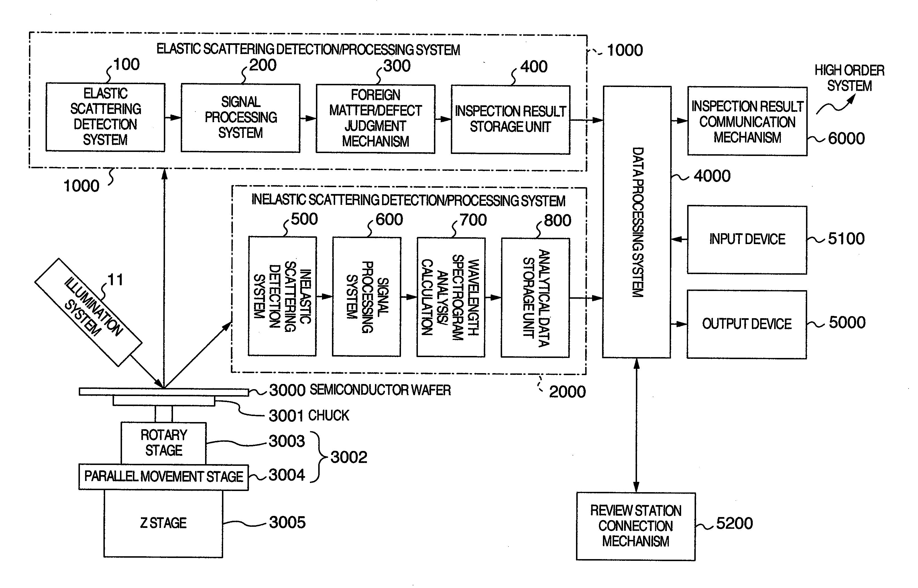
[0044]FIG. 1 shows an inspection device using the inspection method according to the first embodiment of the invention.

[0045]This embodiment will deal an example where micro-defects are detected by removing inelastic scattered light and detecting and processing elastic scattered light.

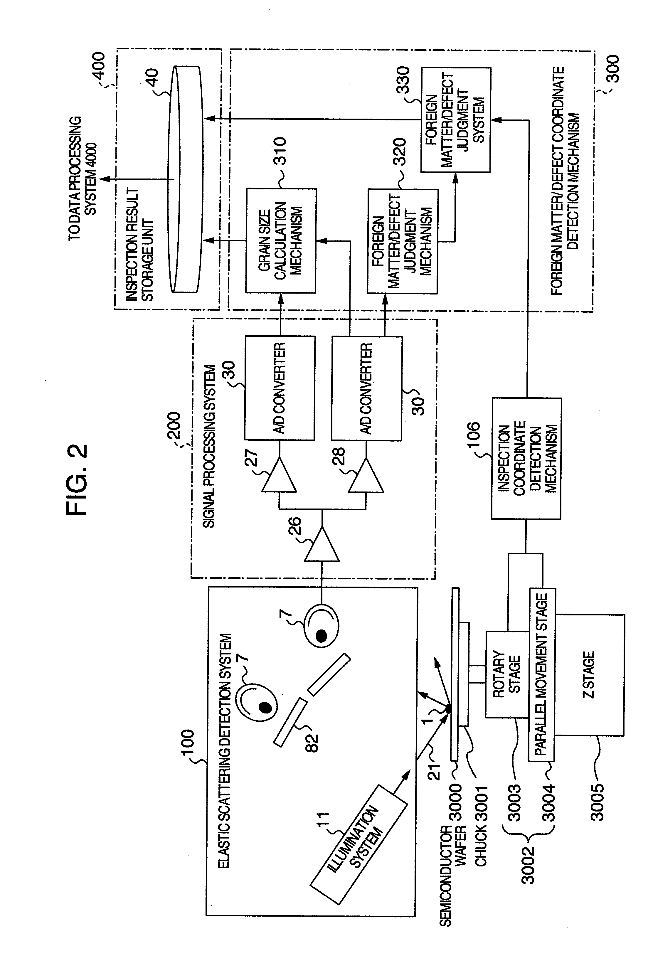
[0046]The surface inspection device includes an inspection object moving stage 3002, a Z stage 3005, an illumination system 11, an elastic scattering detection processing system 1000 and an inelastic scattering detection processing system 2000, a data processing system 4000 for processing information from each processing system, an output device 5000, an input device 5100, a review station connection mechanism 5200 and an inspection result communication mechanism 6000. The semiconductor wafer 3000 as the inspection object is vacuum adsorbed by a chuck 3001. The chuck 3001 is mounted onto the inspection object moving stage 3002 that includes a rotary stage 3003 and a parallel movement stage 3004, and on...

embodiment 2

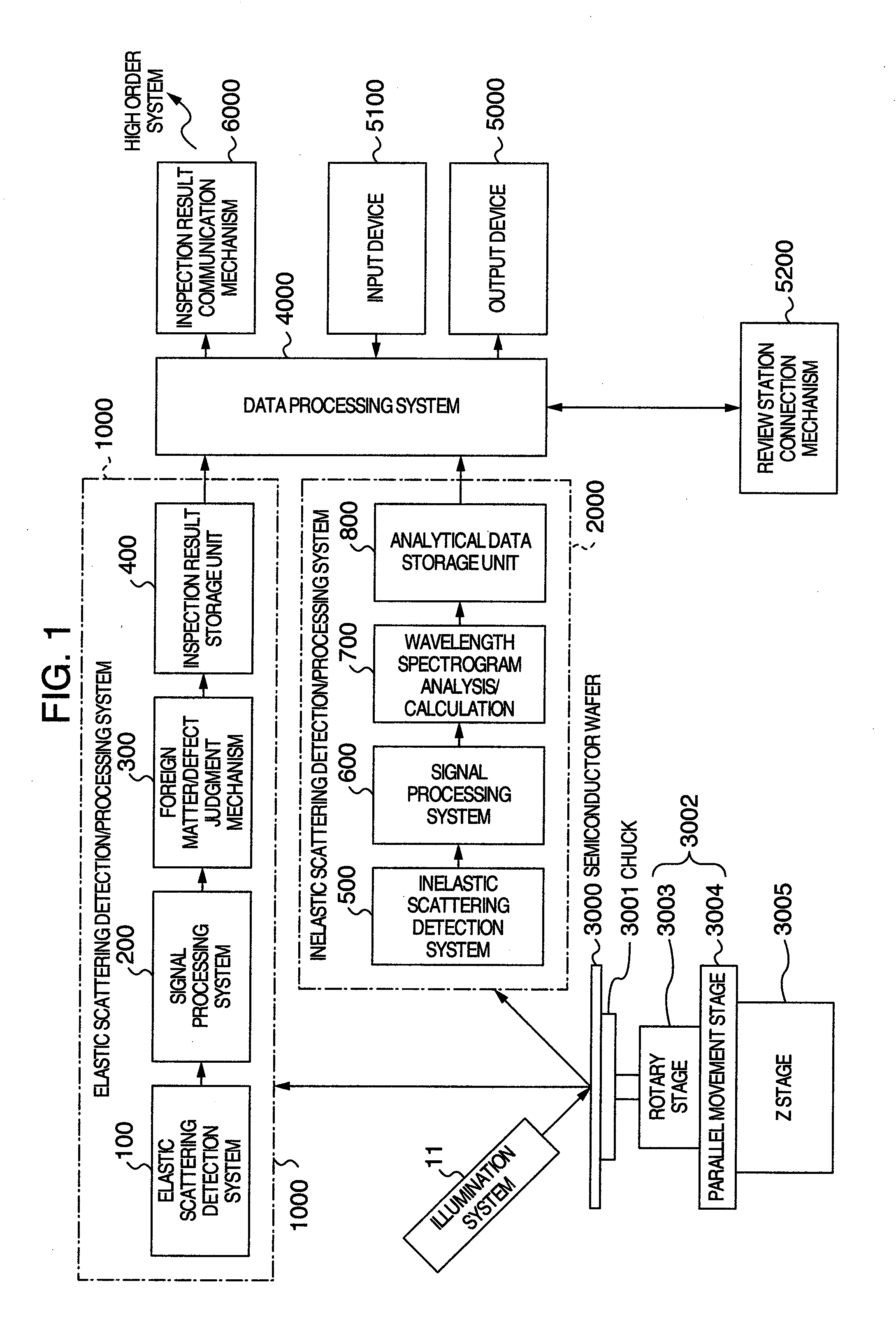
[0118]FIG. 1 shows an inspection device using the inspection method according the second embodiment of the invention. A semiconductor wafer 3000 as an inspection object is vacuum adsorbed to a chuck 3001. The chuck 3001 is mounted onto an inspection object moving stage 3002 and a Z stage 3005 including a rotary stage 3003 and a parallel movement stage 3004.

[0119]The surface inspection device includes an illumination system 11, an elastic scattering detection-processing system 1000 and an inelastic scattering detection-processing system 2000, a data processing system 4000 for processing information from each processing system, an output device 5000, an input device 5100, a review station connection mechanism 5200 and an inspection result communication mechanism 6000.

[0120]Incidentally, the data processing system 4000, the output device 5000, the input device 5100, the review station connection mechanism 5200 and the inspection result communication mechanism 6000 share the data from t...


PUM

PropertyMeasurementUnit
angleaaaaaaaaaa
angleaaaaaaaaaa
wavelengthaaaaaaaaaa

Abstract

An inspection method and an inspection device, or apparatus each capable of conducting composition analysis of a defect detected by elastic or stokes scattered light, an inspection surface or defect on the surface of the inspection surface, or a defect on the surface of the inspection object and its internal composition. A surface inspection method for optically detecting elastic or stokes scattering or inelastic or anti-stokes scattered light from inside the surface of the inspection object, for detecting existence of defects of the inspection object and features of the defects, for detecting positions of the detected defects on the surface of the inspection object, classifying and analyzing the detected defects in accordance with their features on the basis of the positions of the defects and the features of the defects or the classification result of the defects.

Description

BACKGROUND OF THE INVENTION[0001]1. Field of the Invention[0002]This invention relates to an inspection method and an inspection device, or apparatus. For example, the invention is suitable for an inspection method and an inspection method for inspecting defects on surfaces and inside of inspection objects such as semiconductor wafers, magnetic disks, liquid crystal substrates, mask substrates, and so forth.[0003]2. Description of the Related Art[0004]To monitor the dust occurring condition of production apparatuses in a production line of a semiconductor substrate (semiconductor wafer), the inspection of defects such as foreign matters adhering to the surface of the substrate, scratches generated during a processing, etc has so far been carried out. In the case of the semiconductor substrate before the formation of a circuit pattern, for example, fine foreign matters and defects having sizes of not greater than dozens of nm on their surface must be carried out. Besides the foreign ...

Claims


Application Information

Patent Timeline
Patent Type & Authority Applications(United States)
IPC IPC(8): G01N21/88
CPCG01N21/9501G01N21/9505G01N2021/8864G01N2021/4711G01N2021/8861G01N21/65G01N2021/473
Inventor HORAI, IZUOKOYABU, HIROKAZUURANO, YUTAJINGU, TAKAHIRO
Owner HITACHI HIGH-TECH CORP
Why Eureka
Try Eureka