
Ceramic electronic component

a ceramic electronic component and ceramic body technology, applied in the direction of fixed capacitor details, stacked capacitors, fixed capacitors, etc., can solve the problems of reducing mechanical strength, cracking or breaking the ceramic body, cumbersome process, etc., and achieve the effect of high resistan

Active Publication Date: 2009-01-08
TDK CORPARATION
View PDF2 Cites 13 Cited by
  • Summary
  • Abstract
  • Description
  • Claims
  • Application Information

AI Technical Summary

Benefits of technology

[0011]It is an object of the present invention to provide a ceramic electronic component that is sufficiently hard and highly resistant to cracking.
[0012]It is another object of the present invention to provide a ceramic electronic component that is highly resistant to moisture and hardly causes surface leakage current.

Problems solved by technology

At this firing step, there is a problem that mechanical strength is decreased due to insufficient firing of the outermost ceramic layer, easily causing cracking or breaking in the ceramic body.
In the above prior art, however, there is required a cumbersome, complicated process that after formation of the terminal electrode, a glass coating layer is formed by coating with an oxide glass and then the surface of the terminal electrode is exposed by polishing the glass coating layer outside the electrode covering portion of the terminal electrode.
In addition, since the glass coating layer serves as a protective layer, the occurrence of cracking cannot be perfectly prevented because of the nature of glass.
Particularly in recent ceramic electronic components, e.g., a ceramic capacitor, since the distance between the terminal electrodes is extremely shortened due to the rapid progress of miniaturization and slimming down, the surface leakage current easily occurs when an impurity adheres to the ceramic body exposed between the terminal electrodes.

Method used


Image

  • Ceramic electronic component
  • Ceramic electronic component

Examples


Embodiment Construction

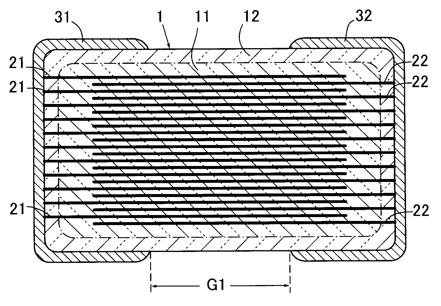
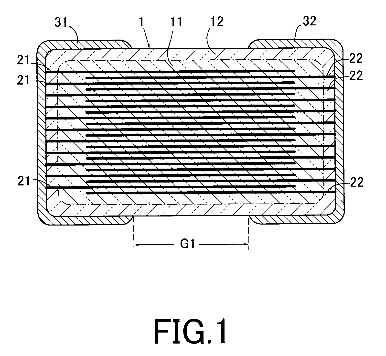
[0027]In FIG. 1, a chip-like ceramic capacitor is shown as a typical example of ceramic electronic components of this type. Other examples include chip inductors, chip filters, chip resistors, chip varistors, and composite ceramic electronic components thereof.

[0028]The illustrated ceramic electronic component has internal electrode layers 21, 22 within a ceramic body 1. Since the present embodiment is a ceramic capacitor, the ceramic body 1 is composed of a BaTiO3 ceramic. The internal electrode layers 21, 22 constitute a pair of capacitor electrode layers whose opposite ends are led to opposite end faces of the ceramic body 1 and connected to terminal electrodes 31, 32 formed thereon. The terminal electrodes 31, 32 are spaced a distance G1 apart from each other, so that the surface of the ceramic body 1 is exposed externally over the distance G1.

[0029]The ceramic body 1 is covered with a diffusion layer 12. The area surrounded by the diffusion layer 12 serves as an originally inte...


PUM


Abstract

A ceramic electronic component includes a ceramic body and an internal electrode layers disposed within the ceramic body. The ceramic body is covered with a diffusion layer, wherein said diffusion layer is an oxide layer into which at least a part of elements contained in the ceramic body are diffused and is located closer to a surface of the ceramic body than an outermost internal electrode layer.

Description

BACKGROUND OF THE INVENTION[0001]1. Field of the Invention[0002]The present invention relates to a ceramic electronic component.[0003]2. Description of the Related Art[0004]Ceramic capacitors are typical examples of ceramic electronic components, wherein a number of internal electrode layers are embedded in a ceramic body composed of, for example, BaTiO3. The internal electrode layers are opposed to each other with an ultrathin ceramic layer interposed therebetween. The ceramic body includes outer layers at both sides in the thickness direction. The outer layers are sufficiently thicker than the ceramic layer interposed between the internal electrode layers. In addition, terminal electrodes that are continuous to the internal electrode layers are attached to both side faces in the length direction. The ceramic body is exposed externally at all the faces other than the side faces with the terminal electrodes attached thereto.[0005]In ceramic electronic components of this type, as des...

Claims


Application Information

Patent Timeline
IPC IPC(8): H01G4/06
CPCH01G4/30H01G4/1227H01G4/12
Inventor IGUCHI, TOSHIHIROYOSHII, AKITOSHIGOSHIMA, AKIRAHASEBE, KAZUYUKI
Owner TDK CORPARATION
Learn More