Method and Apparatus for Packaging an Integrated Chip and Antenna

a technology of integrated chips and antennas, applied in the direction of resonant antennas, waveguide types, feeding systems, etc., can solve the problems of difficult accurate positioning of antennas by consumers, expensive antenna parts, and high cost of antenna components, so as to improve the efficiency of antenna installation and dissipate heat from the chip, the effect of easy and cost-effective manufacturing

Active Publication Date: 2009-01-15
GLOBALFOUNDRIES US INC
View PDF9 Cites 38 Cited by
  • Summary
  • Abstract
  • Description
  • Claims
  • Application Information

AI Technical Summary

Benefits of technology

[0011]Illustrative embodiments of the present invention may be easy and cost effective to manufacture while providing superi

Problems solved by technology

These systems are often assembled using expensive and bulky waveguides and package-level or board-level microstrip structures to interconnect semiconductors and their required transmitter or receiver antennas.
However, because high-gain antennas have very narrow beam widths (thereby making it difficult fo

Method used


Image

  • Method and Apparatus for Packaging an Integrated Chip and Antenna
  • Method and Apparatus for Packaging an Integrated Chip and Antenna
  • Method and Apparatus for Packaging an Integrated Chip and Antenna

Examples


Embodiment Construction

[0022]While reference may be made herein to certain device components, it is to be understood that the present invention is not limited to these or any particular device components or arrangements thereof.

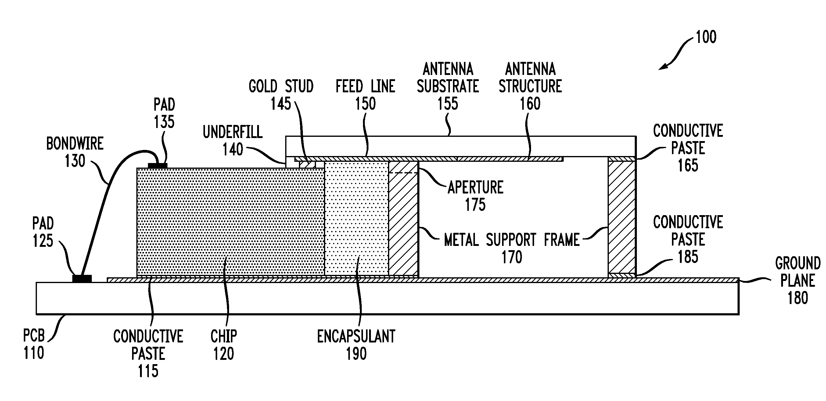
[0023]FIG. 1 shows a package concept with an integrated antenna similar to that described in the Grzyb et al. and Zwick et al. references cited above. This package is well-suited for lab study and testing because of its high performance. For example, an implemented package with a folded dipole antenna of 100 ohms input impedance yields return loss bandwidth more than 30% with efficiency better than 85% and a minimum 7 dBi gain.

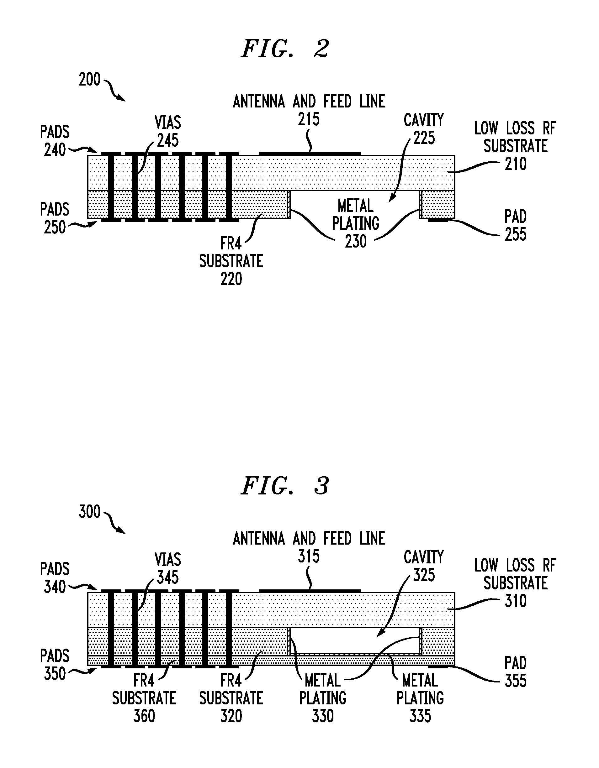
[0024]Although the cost is relatively low for small-scale production, such as that used for the aforementioned lab study and testing, this package requires the use of expensive components such as the substrate with antenna structure and feed line and the metal support frame to form the cavity (etched hole) for the antenna.

[0025]Moreover, packaging the chip an...


PUM


Abstract

In an illustrative embodiment, an apparatus includes at least one antenna structure located on a first surface of a first substrate; at least one pad located on the first surface of the first substrate; and at least one via traversing the first substrate and thereby connecting the at least one pad located on the first surface of the first substrate to at least one pad located on a second surface. The at least one pad located on the first surface of the first substrate is operatively coupleable to at least one pad located on a surface of an integrated circuit and the at least one pad located on the second surface is operatively coupleable to at least one pad located on a surface of a printed circuit board. The at least one via is thereby operative to couple the at least one pad located on the surface of the integrated circuit and the at least one pad located on the surface of the printed circuit board.

Description

CROSS-REFERENCE TO RELATED APPLICATIONS[0001]This application claims the benefit of U.S. Provisional Application No. 60 / 949,884, filed Jul. 16, 2007, and U.S. Provisional Application No. 60 / 949,685, filed Jul. 13, 2007, the disclosures of which are incorporated by reference herein.FIELD OF THE INVENTION[0002]The present invention relates generally to integrated circuit (chip) packaging with integrated antennas or planar phased arrays. Specifically, it is related to chip packaging with integrated antennas or planar phased array designs for millimeter wave (mmWave) frequencies and above.BACKGROUND OF THE INVENTION[0003]In a wireless network, connectivity and communication between devices is achieved through antennas attached to receivers or transmitters in order to radiate the desired signals to or from other elements of the network. In radio communication systems, such as millimeter-wave radios, discrete components are usually assembled with low integration levels. These systems are ...

Claims


Application Information

Patent Timeline
IPC IPC(8): H01Q9/04H01P11/00
CPCH01Q9/0457Y10T29/49016H01Q21/065H01Q21/0006H01L2224/48091H01L2224/73265H01L2924/16195H01L2924/00014
Inventor FLOYD, BRIAN ALLANLIU, DUIXIANMORTON, ROBERT M.
Owner GLOBALFOUNDRIES US INC
Why Eureka
Try Eureka