Sputter coating device and method of depositing a layer on a substrate
a coating device and substrate technology, applied in the direction of electrolysis components, vacuum evaporation coating, coating, etc., can solve the problems of unsatisfactory substrate throughput, low coating yield, and considerable damage to the underlying organic layer
- Summary
- Abstract
- Description
- Claims
- Application Information
AI Technical Summary
Benefits of technology
Problems solved by technology
Method used
Image
Examples
first embodiment
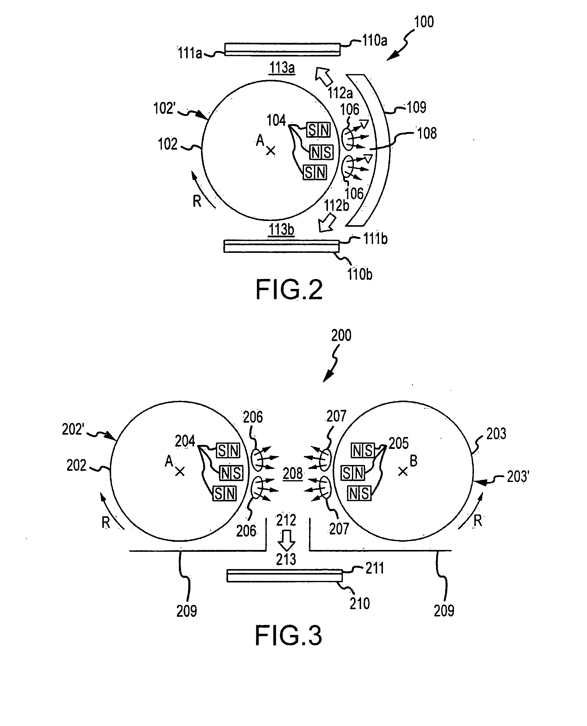
[0058]FIG. 2 illustrates a sputter coating device 100 according to the present invention. The sputter coating device 100 comprises a vacuum coating chamber (not illustrated), and substrates 110a and 110b arranged within the coating chamber. Furthermore, the sputter coating device 100 comprises a cylindrical hollow cathode including a rotatable target 102 rotating around a central axis A, and a magnet assembly 104 which is arranged within the hollow cathode and arranged such that confining plasma zones 106 are generated in an area 108 above the surface 102′ of the target 102. The area 108 is arranged such that the prevailing direction of movement of particles sputtered from the surface 102′ of the target 102 is not directed toward the substrate surface to be coated.
[0059]In this embodiment, there are two substrates 110a and 110b to be coated at the same time. Both substrates have an OLED layer 111a and 111b, respectively, deposited on the substrate surface. However, it is also possib...
second embodiment
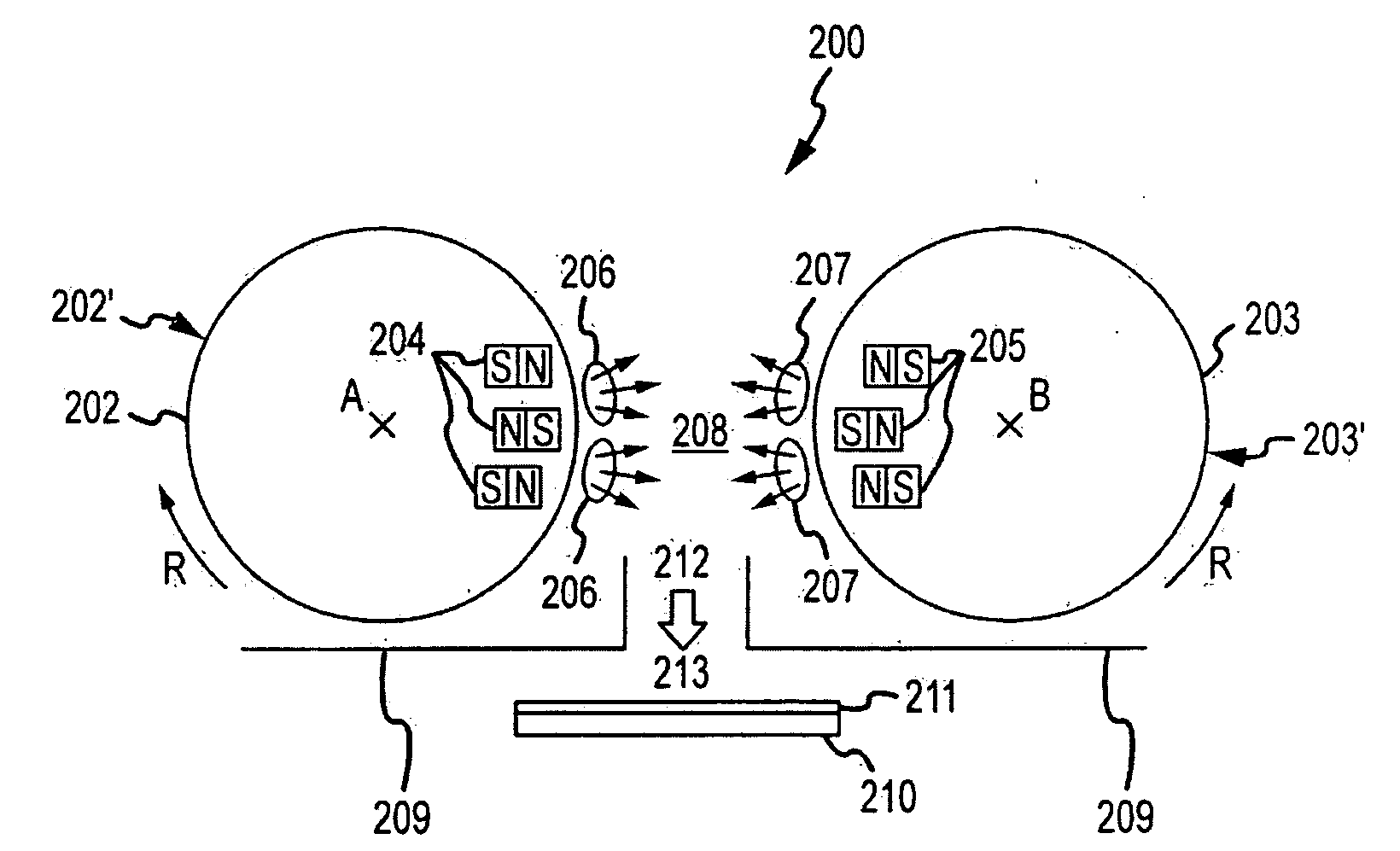
[0063]FIG. 3 is an illustration of the inventive sputter coating device 200. The second sputter coating device 200 comprises a vacuum coating chamber (not illustrated), a first rotatable cathode having a first target 202, and a second rotatable cathode having a second target 203. The targets 202 and 203 are rotatable around central axes A and B, respectively. Furthermore, the first and second cathodes 202 and 203 comprise a magnet assembly 204 and 205, respectively. The magnets 204 and 205 are arranged such that two plasma confinement zones 206 and 207 are generated in a defined area between the targets 202 and 203.
[0064]The plasma confinement zones 206 and 207 are positioned in an intermediate space 208 between the targets 202 an 203. The particles sputtered from the target surfaces 202′ and 203′ in an area near the plasma confinement zones 206 and 207 have a prevailing direction of movement toward the other rotatable cathodes 203 and 202, respectively. The magnet assemblies, 204, ...
PUM
| Property | Measurement | Unit |
|---|---|---|
| thickness | aaaaa | aaaaa |
| thickness | aaaaa | aaaaa |
| thickness | aaaaa | aaaaa |
Abstract
Description
Claims
Application Information


