Method for fabricating semiconductor device
- Summary
- Abstract
- Description
- Claims
- Application Information
AI Technical Summary
Benefits of technology
Problems solved by technology
Method used
Image

Examples
embodiment 1
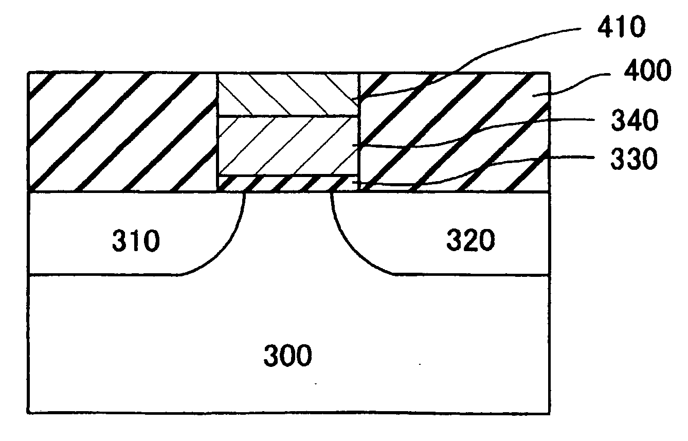
[0068]In this embodiment, when a transistor is to be formed on a semiconductor substrate, at the step of introducing an impurity for forming a source / drain region, the impurity is introduced into a silicon substrate surface having a gate electrode formed, by a plasma doping using the gate electrode as a mask. The embodiment is characterized by the step of forming a reflection preventing film, before the impurity is activated by an optical irradiation, so that the optical reflectivity of the region having said impurity introduced thereinto may become low.
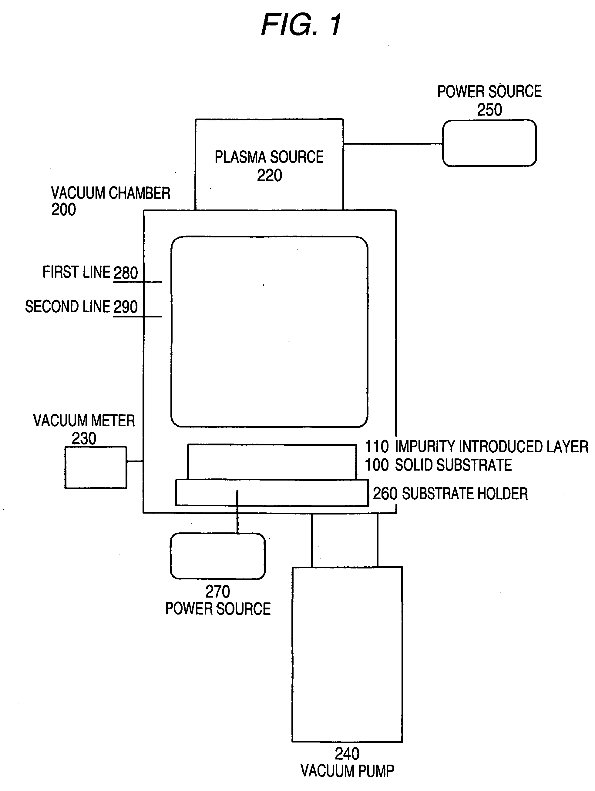
[0069]Prior to the description of the process, here are described at first a plasma doping apparatus and an impurity doping process, which are used in a semiconductor device fabricating method used in this embodiment. The doping apparatus to be used in this embodiment is provided, as shown in FIG. 1, with a vacuum chamber 200 and a plasma source 220 for exciting a plasma in the vacuum chamber 200. The doping apparatus performs a plas...
embodiment 2
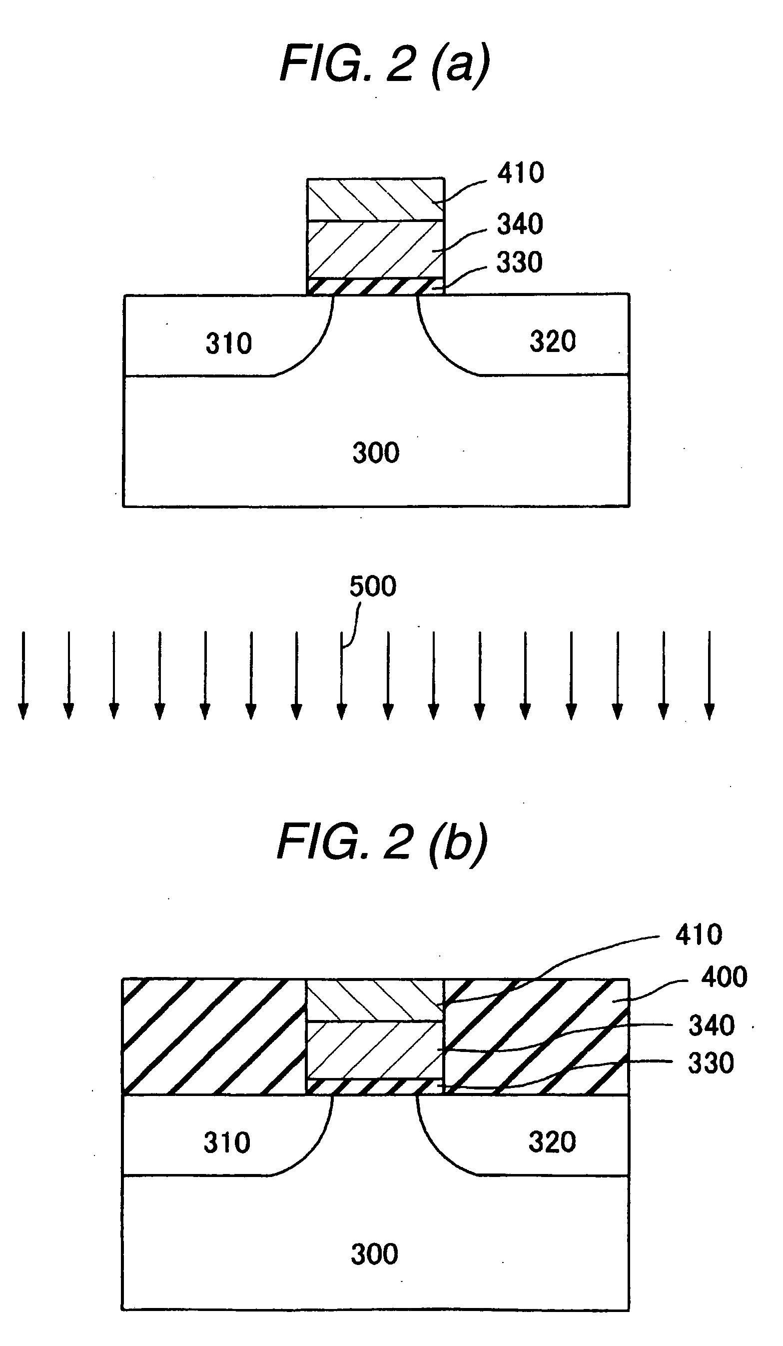
[0079]Next, Embodiment 2 of the invention is described. FIGS. 3(a) to (c) are schematic diagrams showing a method of Embodiment 2. In Embodiment 1, the annealing is performed by forming the reflecting film on the gate electrode surface and by forming the silicon oxide film as the reflection preventing film on the semiconductor substrate surface to become the source / drain region. In this embodiment, the reflection preventing film 400 is formed not only on the gate electrode but also on the semiconductor substrate to become the source / drain region, and is made thinner on the gate electrode so that it reduces the optical absorption on the gate electrode thereby to suppress the temperature rise at the gate electrode portion and the melting of the gate.
[0080]The gate oxide film 330 made of a silicon oxide film and the gate electrode 340 made of a toped crystal silicon film are formed on the surface of the silicon substrate 300. At this time, the patterning of the gate electrode is perfor...
embodiment 3
[0090]Next, in Embodiment 3 of the invention, the step of making amorphous is executed before the step of introducing the impurity by the plasma. As a result, it is possible to raise the optical absorptivity of the region having the impurity introduced thereinto.
[0091]In this embodiment, before the step of introducing the impurity by the plasma, i.e., the plasma doping step, the surfaces of the regions to have the impurity introduced thereinto are made amorphous in advance to lower the reflectivities. Specifically, the regions are individually made amorphous by the He plasma (as expressed by He—PA) and by the Ge ion injection (as expressed by Ge—PA), and the silicon oxide film is then formed as the reflection preventing film. Subsequently, the doping is performed as in the aforementioned Embodiments 1 and 2. The remaining procedures are similar to those of the aforementioned Embodiments 1 and 2.
[0092]In FIG. 5, the relations of the reflectivities against the individual wavelength of...
PUM
 Abstract
Description
Claims
Application Information
 - R&D Engineer
- R&D Manager
- IP Professional
- Industry Leading Data Capabilities
- Powerful AI technology
- Patent DNA Extraction
Browse by: Latest US Patents, China's latest patents, Technical Efficacy Thesaurus, Application Domain, Technology Topic.
© 2024 PatSnap. All rights reserved.Legal|Privacy policy|Modern Slavery Act Transparency Statement|Sitemap