Semiconductor memory device and driving method thereof

a memory device and semiconductor technology, applied in the direction of static storage, digital storage, instruments, etc., can solve the problems of corrupted stored data, reduced storage node potential vb>1/b>, and caused corruption of stored data, so as to reduce leakage current, enlarge read margin, and reduce leakage current

Active Publication Date: 2009-01-29
NEC CORP
View PDF1 Cites 46 Cited by
  • Summary
  • Abstract
  • Description
  • Claims
  • Application Information

AI Technical Summary

Benefits of technology

[0047]A memory cell in a semiconductor memory device according to the present invention has first and second inverter circuits forming first and second data storage nodes with loop connection, first and second access portions operable to access the first and second data storage nodes, respectively, and a holding control portion connected in series with a drive transistor of the second inverter circuit. The memory cell is configured to switch a low power source potential by a low potential switching portion provided between the low power source potential of the first inverter circuit and a ground potential or provided between the low power source potential of the first and second inverter circuits and a ground potential. Thus, it is possible to obtain effects of reducing a leakage current and enlarging a write margin.
[0048]Furthermore, in the memory cell, an off period and a read activation period of the holding control portion are controlled by using a signal having a pulse width equal to a reading ti...

Problems solved by technology

However, in a conventional SRAM cell, a problem of corruption of stored data also arises when a reading operation is performed at a low power source voltage.
However, because a drive transistor N1 is in an on state, it lowers the potential of the storage node V1.
As a result, corruption of the stored data is caused.
When an SNM is 0 mV or less, stored data ...

Method used


Image

  • Semiconductor memory device and driving method thereof
  • Semiconductor memory device and driving method thereof
  • Semiconductor memory device and driving method thereof

Examples


first example

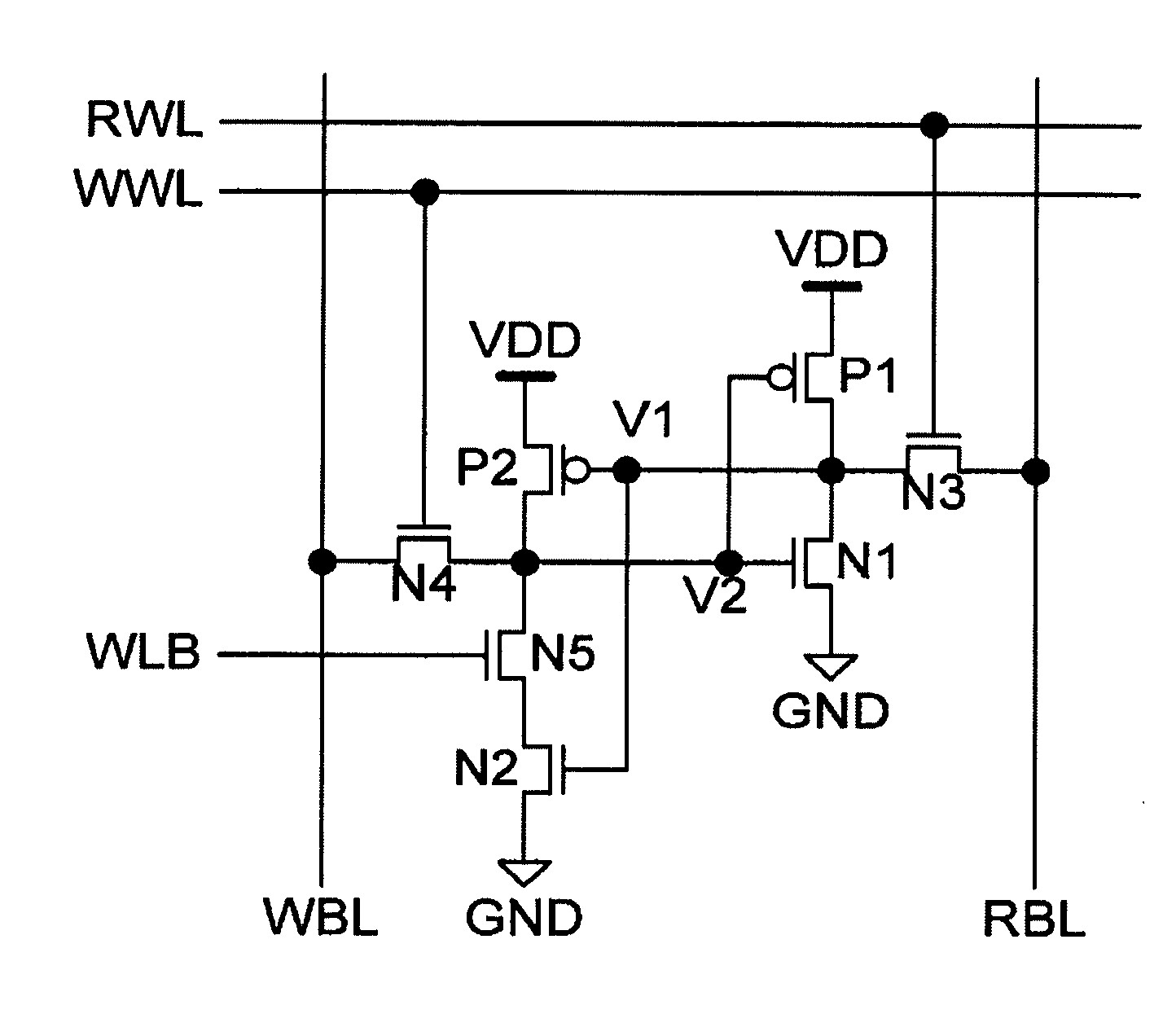
[0100]A first example will be described with reference to FIGS. 9 to 13. A semiconductor device in the first example employs SRAM cells each formed by seven transistors as shown in FIG. 5. In order to more reliably hold data of the SRAM cells in a reading operation, an off time of the holding control transistors is set to be equal to a minimum pulse width to thereby prevent corruption of holding data of the SRAM cells.

[0101]FIG. 9 shows a block arrangement explanatory of a flow of signals, and FIG. 10 shows a replica block. FIG. 11 shows operation waveforms of the replica block, and FIG. 12 shows operation waveforms of an SRAM block and an SRAM cell. FIG. 13 shows a multiplexed replica block.

[0102]In the semiconductor memory device 1 shown in FIG. 9, blocks 2 each having an SRAM cell of m words and n bits are arranged in the form of an M×N matrix. Each block has a sub-word driver and a sense amplifier (not shown). The sub-word driver is operable to activate a word line selected by a...

second example

[0118]A second example will be described with reference to FIGS. 14A, 14B, and 15A to 15C. In the second example, a leakage current of the storage node V2 is controlled in a reading operation so as to hold data of the storage node V2. The level of a low potential “0” of the inverse word line signal WLB, which is a control signal for the holding control transistor N5 in the SRAM cell, is set to be 0.1V to 0.2V higher than the ground potential GND so as to increase a leakage current Ioff_N5 of the transistor N5. In this manner, a leakage current of the storage node V2 is set to have the relationship of Ioff_N4+Ioff_N5>>Ioff_P2. Thus, stored data are held.

[0119]A flow of signals between blocks will be described with reference to FIGS. 14A and 14B. FIG. 14A shows a block arrangement explanatory of a flow of signals, and FIG. 14B shows operation waveforms. In the semiconductor memory device 1, blocks 2 each having an SRAM cell of m words and n bits are arranged as a cell array in the for...

third example

[0124]A third example will be described with reference to FIGS. 16A, 16B, 17A, and 17B. In the third example, an off-state leakage current of the access transistor N4 connected to the write bit line WBL in the SRAM cell is controlled to hold data of the storage node V2. At the time of reading from the SRAM cell, the write word line signal WWL has a low potential “0”, so that the access transistor N4 is in an off state. In the third example, the level of a low potential “0” of the write word line signal WWL is set to be 0.1V to 0.2V higher than the ground potential GND so as to increase a leakage current Ioff_N4 of the access transistor N4. In this manner, a leakage current of the storage node V2 is set to have the relationship of Ioff_N4+Ioff_N5>>Ioff_P2. Thus, stored data are held.

[0125]FIG. 16A shows an arrangement of a block 2, and FIG. 16B shows a circuit of a sub-word driver. FIG. 17A shows a generation circuit for the write word line signal WWL, and FIG. 17B shows operation wa...


PUM


Abstract

In a reading operation, an off time and a reading time of a holding control transistor is controlled by a replica circuit, so that a read margin is enlarged. Furthermore, a high power source potential and a low power source potential of an SRAM memory cell are switched in reading and writing operations of the memory cell and in a data holding state by a power source potential switching portion. As a result, a write margin is enlarged, and a leakage current is reduced.

Description

TECHNICAL FIELD[0001]The present invention relates to a semiconductor memory device, and more particularly to a semiconductor memory device capable of operating at an ultrahigh speed and an ultralow voltage with a memory cell formed by seven transistors and a driving method thereof.BACKGROUND ART[0002]Recent semiconductor devices have not only been scaled up and speeded up, but also been systematized by incorporating many functions. In order to scale up and speed up semiconductor devices, transistors have been made finer, and operating speeds have been improved while power source voltages have been reduced. Various types of function blocks including CPUs and various types of memory devices are combined with each other for systematization. Those memory devices jointly mounted on system LSIs are similarly required to operate at a high speed and a low power source voltage. For example, a static random access memory (hereinafter abbreviated as an SRAM), which is jointly mounted for appl...

Claims


Application Information

Patent Timeline
IPC IPC(8): G11C11/412G11C7/00G11C5/14
CPCG11C11/412H01L27/1104H01L27/092G11C11/417H10B10/12
Inventor TAKEDA, KOICHI
Owner NEC CORP
Why Eureka
Try Eureka