

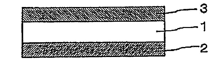
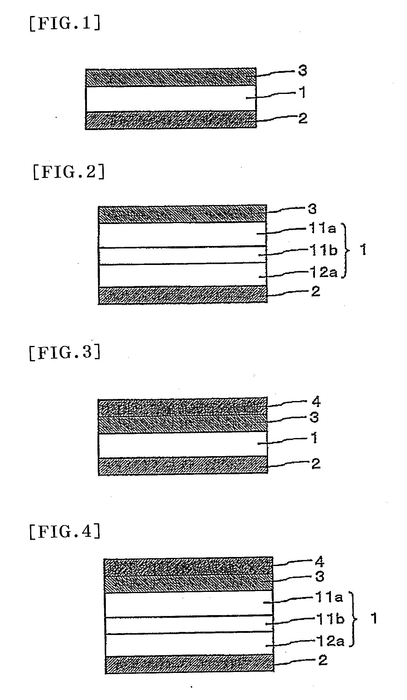
Transparent conductive film and touch panel
a technology of transparent conductive film and touch panel, which is applied in the direction of instruments, other domestic objects, transportation and packaging, etc., can solve the problems of inability to use certain purposes, short life of touch panel, and low flexibility or workability, and achieve good scratch resistance
- Summary
- Abstract
- Description
- Claims
- Application Information
AI Technical Summary
Benefits of technology
Problems solved by technology
Method used
Image

Examples
example 1
Formation of Conductive Thin Layer
[0106]A transparent conductive thin layer made of a 25 nm-thick ITO film (2.00 in refractive index) was formed on one side of a 25 μm-thick polyethylene terephthalate film (PET Film 1) by a reactive sputtering method using a sintered material composed of 90% by weight of indium oxide and 10% by weight of tin monoxide in a 4×10³ Torr atmosphere composed of 80% argon gas and 20% oxygen gas.
(Hard Coat Material)
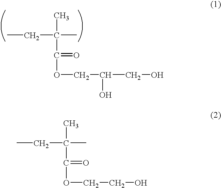
[0107]A hard-coating material was prepared using the following materials: a urethane acrylate (hereinafter referred to as Component A) (100 parts of a urethane acrylate produced with pentaerythritol acrylate and hydrogenated xylene diisocyanate); polyol (meth)acrylate (hereinafter referred to as Component B) (49 parts of dipentaerythritol hexaacrylate (hereinafter referred to as Component B1 (monomer)), 41 parts of pentaerythritol tetraacrylate (hereinafter referred to as Component B4 (monomer)) and 24 parts of pentaerythritol triacrylate (herein...
example 2
[0111]In the process according to Example 1, 30 parts of PMMA particles (1.49 in refractive index) with an average particle size of 10 μm were added to the total amount of the resin components, when the hard coating material was prepared. A transparent conductive laminate and a touch panel were prepared using the process of Example 1, except that the resulting hard coating material was used instead.
examples 3 to 8
[0112]Transparent conductive laminates and touch panels were prepared using the process of Example 2, except that the amount of the addition of fine particles, the average particle size, and the thickness of the hard-coating layer were changed as shown in Table 1.
PUM
| Property | Measurement | Unit |
|---|---|---|
| thickness | aaaaa | aaaaa |
| particle size | aaaaa | aaaaa |
| thickness | aaaaa | aaaaa |
Abstract
Description
Claims
Application Information