

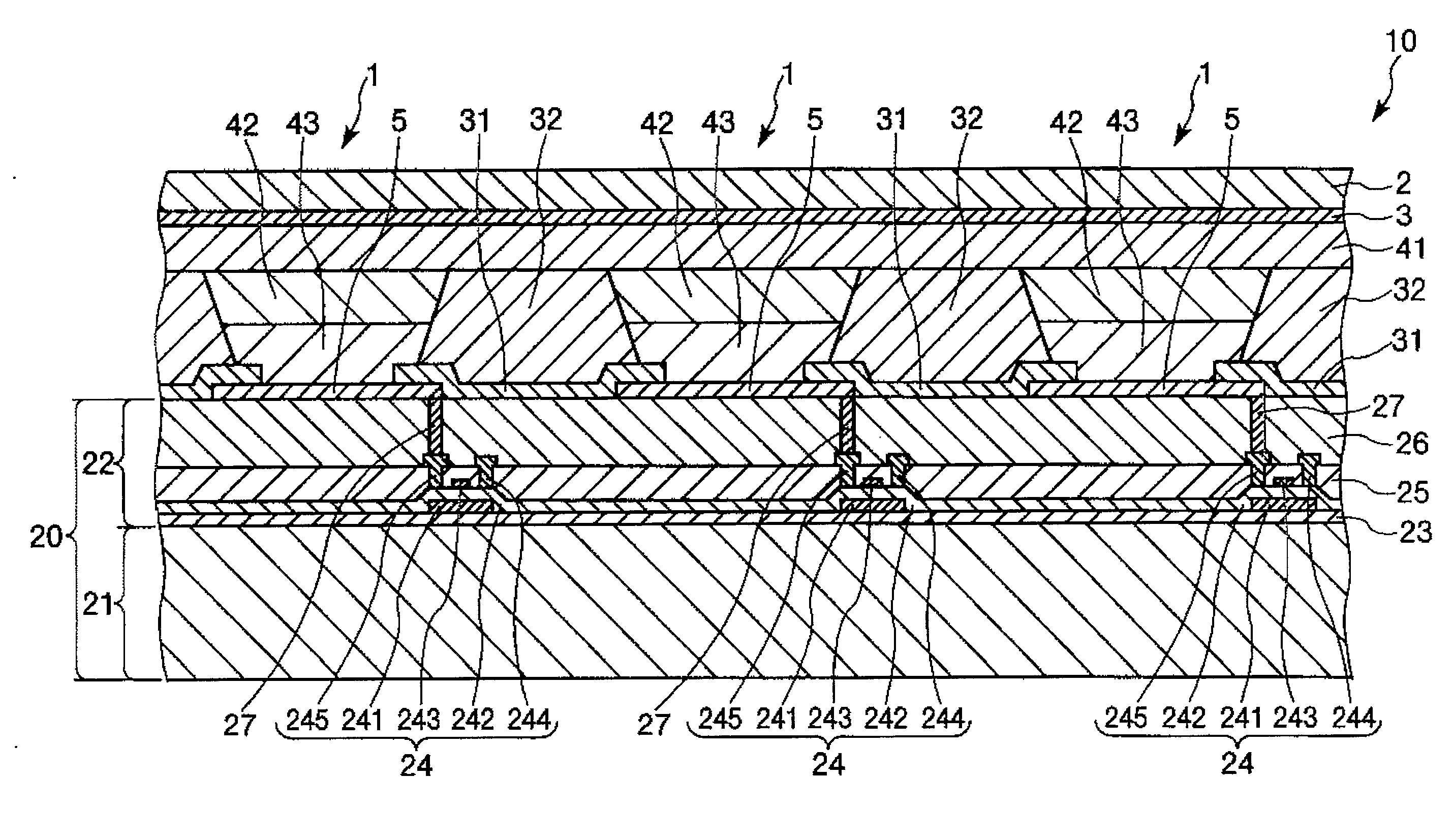
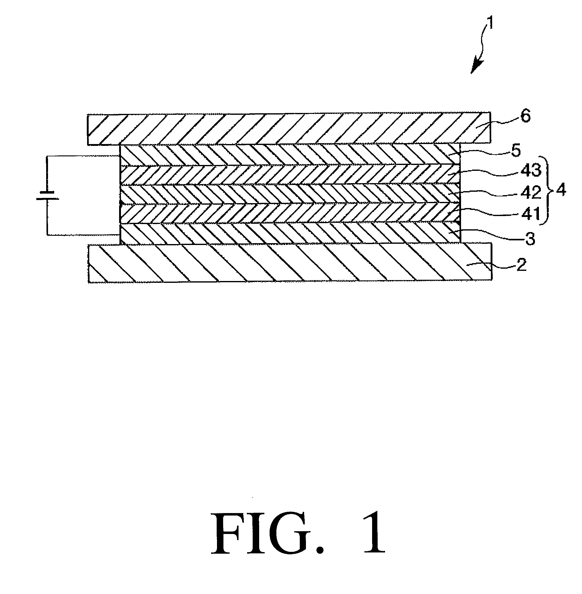
Method of Manufacturing Semiconductor Element, Semiconductor Element, Electronic Device, and Electronic Equipment
- Summary
- Abstract
- Description
- Claims
- Application Information
AI Technical Summary
Benefits of technology
Problems solved by technology
Method used
Image

Examples
example 1
Preparation of Hole Transport Layer Formation Material
[0342]The compound (A) was used as the hole transport material and isophthalic hydrazide was used as a heat polymerization initiator, and the compound (A) and the isophthalic hydrazide in a weight ratio of 50:1 were mixed in a xylene solution to prepare a hole transport layer formation material.
[0343]
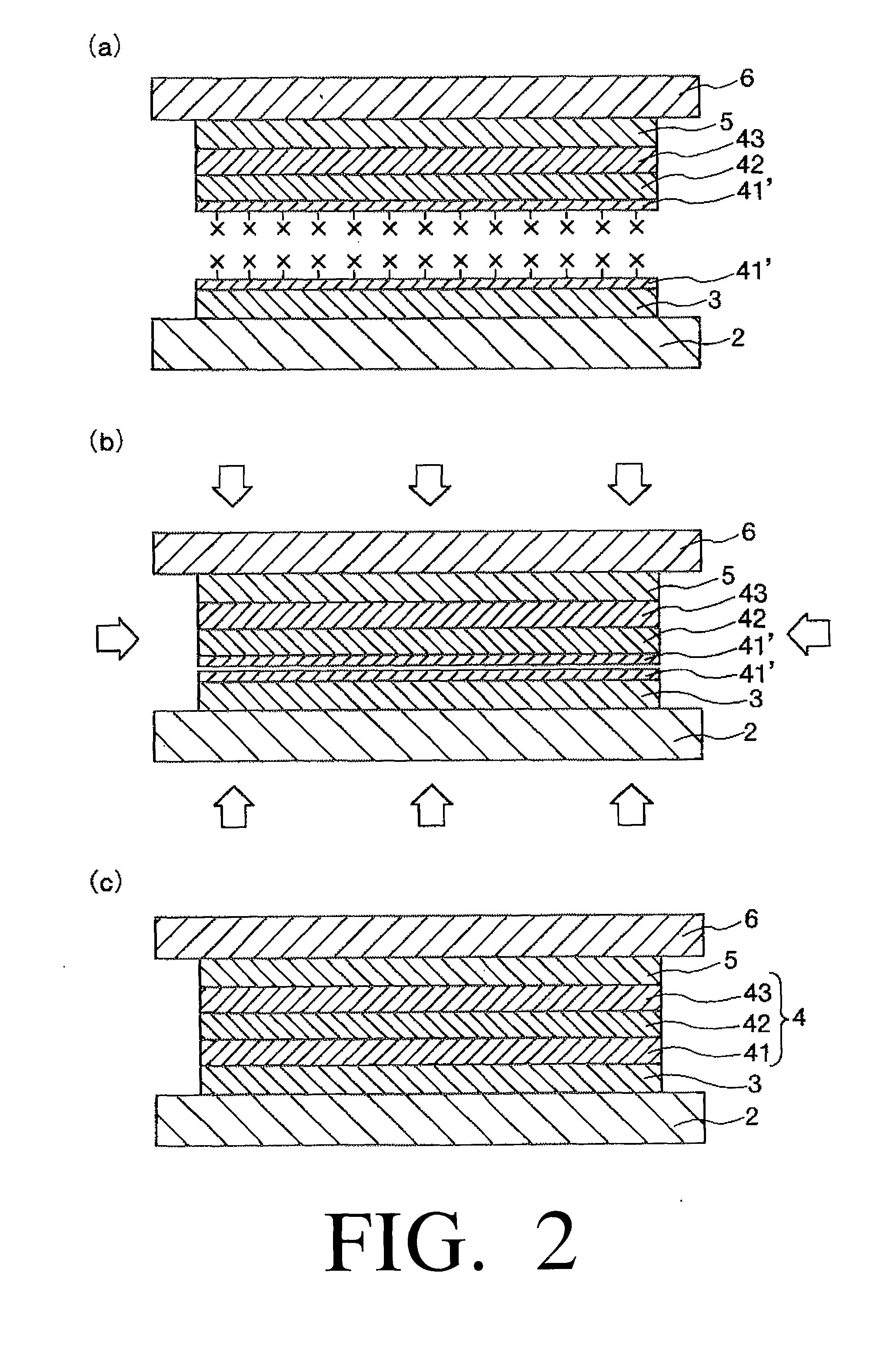
[0344]1A First, an ITO electrode (that is, an anode) was formed on a transparent glass substrate having an average thickness of 0.5 mm by vacuum evaporation so as to have an average thickness of 100 nm.
[0345]2A Next, the hole transport layer formation material was applied onto the ITO electrode by a spin coating method, and then the solvent was removed to form a coating layer.
[0346]3A Next, the thus formed coating layer was subjected to a heat treatment in an atmosphere at a temperature of 100° C. for 30 minutes so that the coating layer became a semi-solid state.
[0347]4A Next, an AlLi electrode (that is, a cathode) was formed on a t...
example 2
Preparation of Hole Transport Layer Formation Material
[0355]The compound (A) was used as the hole transport material, diethylenetriamine was used as a curing agent, and isophthalic hydrazide was used as a heat polymerization initiator, and they were mixed in a xylene solution to prepare a hole transport layer formation material.
[0356]The mixing ratio of the compound (A) and the diethylenetriamine in a weight ratio was 10:1, and the weight ratio of the total weight of the compound (A) and the diethylenetriamine and the weight of the isophthalic hydrazide was 50:1.
[0357]
[0358]Organic EL devices were manufactured in the same manner as in the Example 1 except that the hole transport layer formation material obtained in this Example was used for the formation of the coating layers in the above steps 2A and 7A, that the heat treatment in the above step 3A was carried out in an atmosphere at a temperature of 80° C. for 5 minutes, that the heat treatment in the above step 8A was carried out...
example 3
[0359]Organic EL devices were manufactured after the hole transport material was prepared in the same manner as in the Example 1 except that the compound (B) was used as the hole transport material. Each of the thus manufactured organic EL devices had a structure shown in the following Table 3.
TABLE 3Order ofElectrodes andConstituentSubstrateLaminationSemiconductor LayersMaterialGlass1CathodeAlLiSubstrate2Electron Transport LayerCompound (G)3Light Emitting LayerCompound (H)4Layer to be IntegratedCompound (B)(Layer Formed by Integration of Layers: Hole Transport Layer)Glass2Layer to be IntegratedCompound (B)Substrate1AnodeITO
PUM
| Property | Measurement | Unit |
|---|---|---|
| Carrier mobility | aaaaa | aaaaa |
| Temperature | aaaaa | aaaaa |
| Degree of polymerization | aaaaa | aaaaa |
Abstract
Description
Claims
Application Information