Optical Measurement Apparatus and Method
a measurement apparatus and optical technology, applied in the direction of optical radiation measurement, instruments, spectrometry/spectrophotometry/monochromators, etc., can solve the problems of slow measurement speed, preventing widespread industrial application, and affecting the measurement accuracy
- Summary
- Abstract
- Description
- Claims
- Application Information
AI Technical Summary
Problems solved by technology
Method used
Image
Examples
example
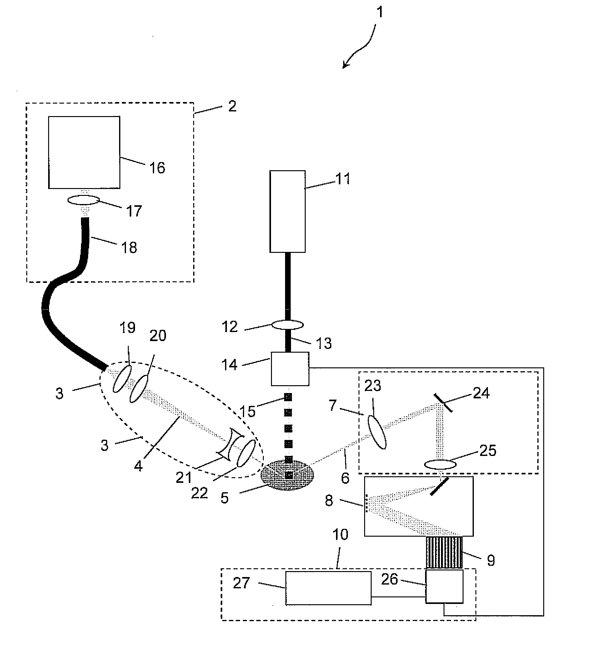
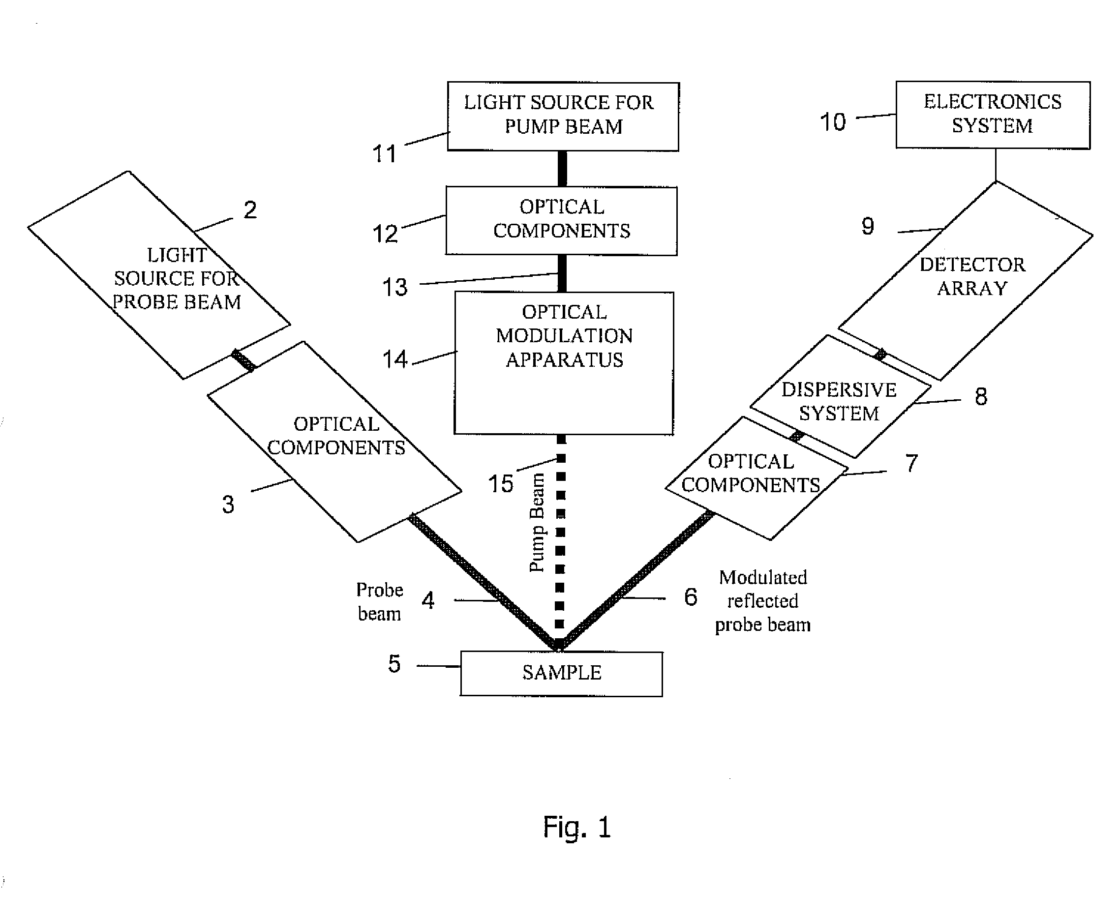
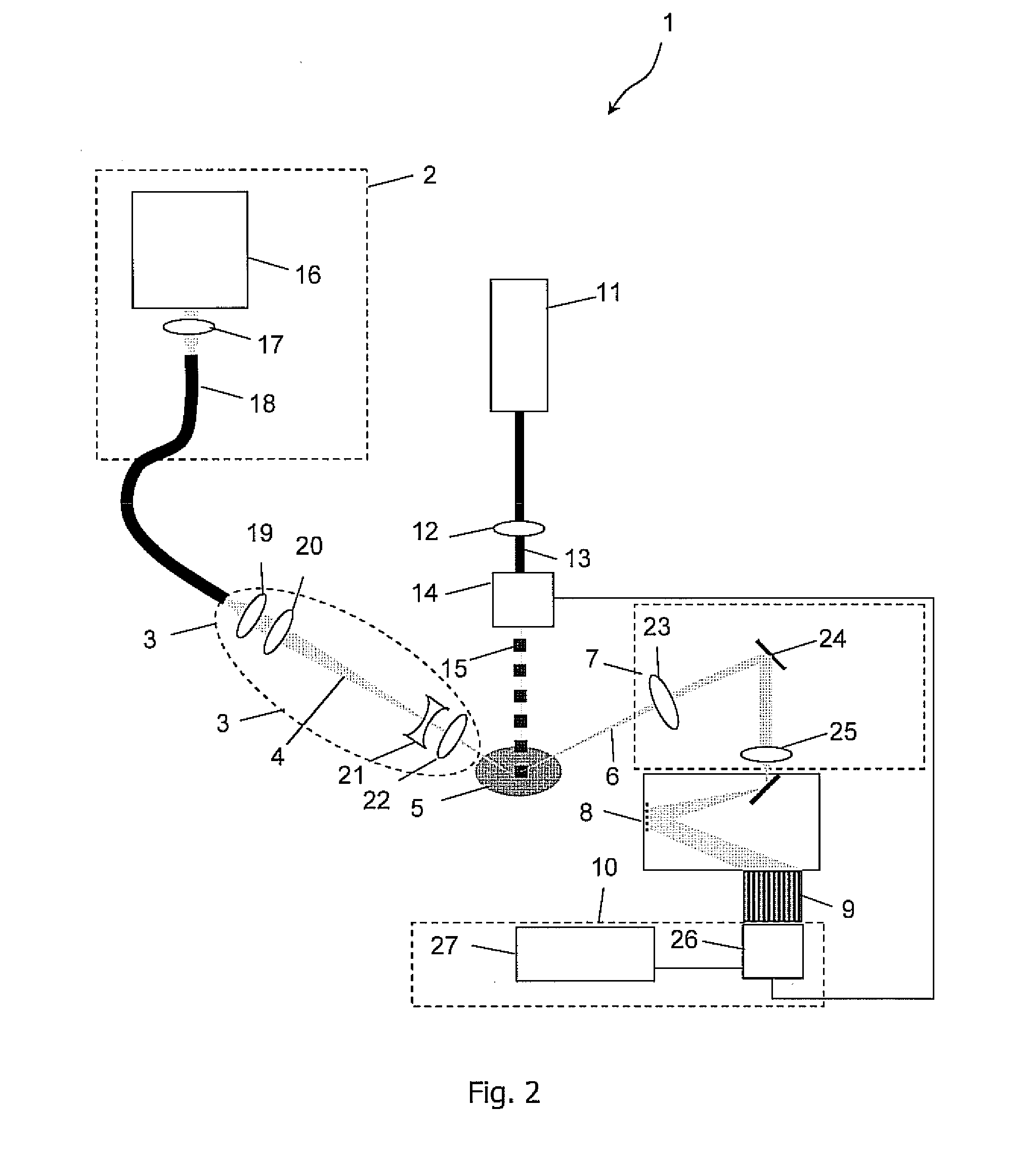
[0190]The following examples are not intended to limit the scope of the invention. In one specific example of the invention, a 300 W Oriel 6258 Ozone-Free Xenon arc lamp was used with reflecting and light collecting to produce a blue and near ultraviolet probe light beam, which was collimated and reflected from a silicon wafer and coupled to an Andor Shamrock SR303i Imaging Spectrograph, fitted with a grating with 600 lines per mm and blazed at 300 nm. To the exit port of the spectrograph was mounted a Hamamatsu S3921-512Q photodetector array. A Coherent 315M 150 mW diode-pumped solid state laser was amplitude modulated at a chopping frequency of 139 Hz using an Ametek optical chopper, and shone over the area of incidence of the probe light beam. A driver circuit designed for the S3921-512Q photodetector array was connected behind the array, and a special circuit designed to lengthen the output video-signal-type pulses from the array and driver circuit, was electrically connected to...
example application
[0194]In one specific example of the invention, the photoreflectance spectrum of a strained silicon layer grown pseudomorphically on a silicon-germanium alloy of Ge alloy mole fraction 20.4%, is measured over the spectral range 2.8 eV to 3.6 eV at intervals of 0.002 eV. The spectrum is fitted to a summation of two low field photoreflectance lineshapes of the form of expression 1 above, and found to have an E1+ transition energy of 3.287 eV, shifted 105 meV from the E1 transition energy of 3.392 eV of unstrained bulk silicon on the substrate of the same wafer. The shifts ΔE in each branch of the split E1 transition energy and their relationship to the in-plane and out-of-plane strain tensor elements ∈⊥ and ∈∥ may be written in the form 3:
ΔE=−3.267(∈⊥+2∈∥)±1.567(∈⊥−∈∥) 3
where the “±” sign is applied as “+” to obtain the shift in the E1+ branch and as “−” to obtain the shift in the E1− branch, from the E1 transition energy of unstrained silicon. Converted to in-plane strain using the ...
PUM
| Property | Measurement | Unit |
|---|---|---|
| optical modulation spectroscopy | aaaaa | aaaaa |
| wavelengths | aaaaa | aaaaa |
| reflectance | aaaaa | aaaaa |
Abstract
Description
Claims
Application Information


