Structure and process for production thereof
a technology of structure and process, applied in the field of structure, can solve the problems of thermal fluctuation to render the recording magnetization instable, reduce the recording performance of the recording head, and reduce the effective recording magnetic field intensity, and achieve the effect of high recording sensitivity
- Summary
- Abstract
- Description
- Claims
- Application Information
AI Technical Summary
Benefits of technology
Problems solved by technology
Method used
Image
Examples
example 1
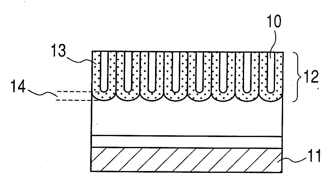
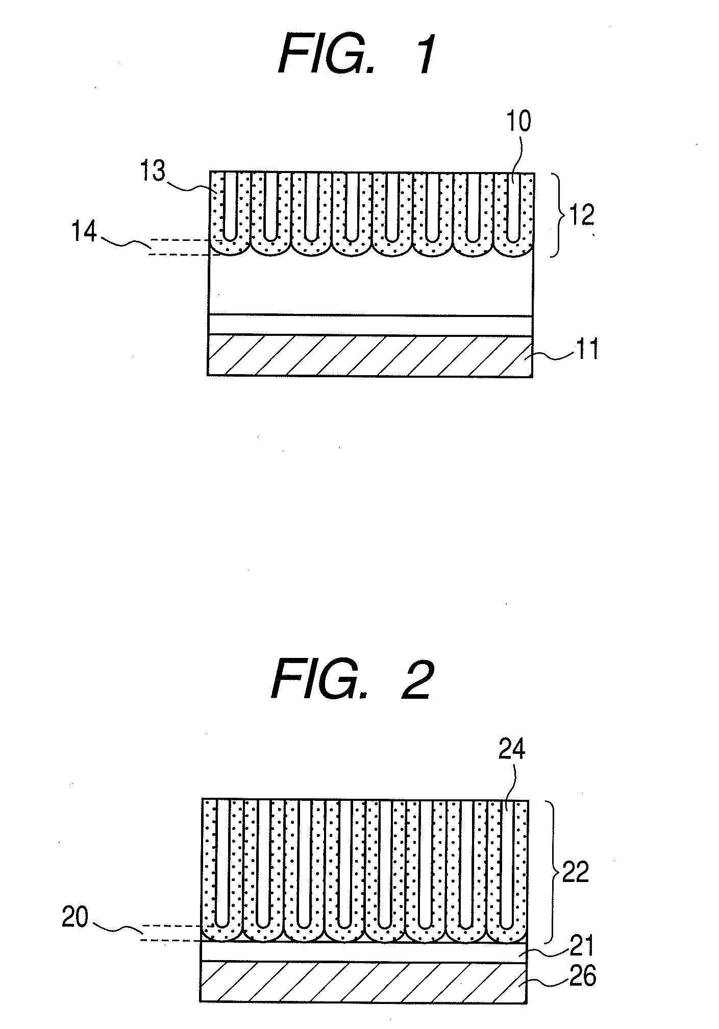
[0085]A Ti film of 5-nm thick, a Nb film of 20-nm thick as an underlying metal layer, and an AlHf layer of 35-nm thick containing Hf at a content of 7 atom % are formed, on a Si substrate successively by sputtering. On the AlHf surface, small dents are formed in a square array at dent intervals of 25 nm as the anodization initiation points by an FIB process. The surface AlHf layer is anodized in an aqueous 1.0-mol / L sulfuric acid solution at a bath temperature of 3° C. at an anodization voltage of 10 V. The resulting porous film layer is wet-etched for pore-widening in an aqueous 5-wt % phosphoric acid solution at a bath temperature of 20° C. The pore diameter is found to be 12 nm by observation of the surface of the workpiece by FE-SEM.
[0086]The workpiece is further anodized in an aqueous 0.15-mol / L ammonium borate solution at a bath temperature of 22° C. at an anodization voltage of 19 V. Thereby, an oxide of the underlying Nb grows and expands into the pores to fill the pores as ...
example 2
[0088]A Ti film of 5-nm thick, a Ta film of 20-nm thick as an underlying metal layer, and an AlHf layer of 35-nm thick containing Hf at a content of 7 atom % are formed, on a Si substrate successively by sputtering. On the AlHf surface, small dents are formed in a square array at dent intervals of 25 nm as the anodization initiation points by an FIB process. The surface AlHf layer is anodized in an aqueous 1.0-mol / L sulfuric acid solution at a bath temperature of 3° C. at an anodization voltage of 10 V. The resulting porous film layer is wet-etched for pore-widening in an aqueous 5-wt % phosphoric acid solution at a bath temperature of 20° C. The pore diameter is found to be 12 nm by observation of the surface of the workpiece by FE-SEM.
[0089]The workpiece is further anodized in an aqueous 0.15-mol / L ammonium borate solution at a bath temperature of 22° C. at an anodization voltage of 19 V. Thereby, an oxide of the underlying Ta grows and expands into the pores to fill the pores wit...
example 3
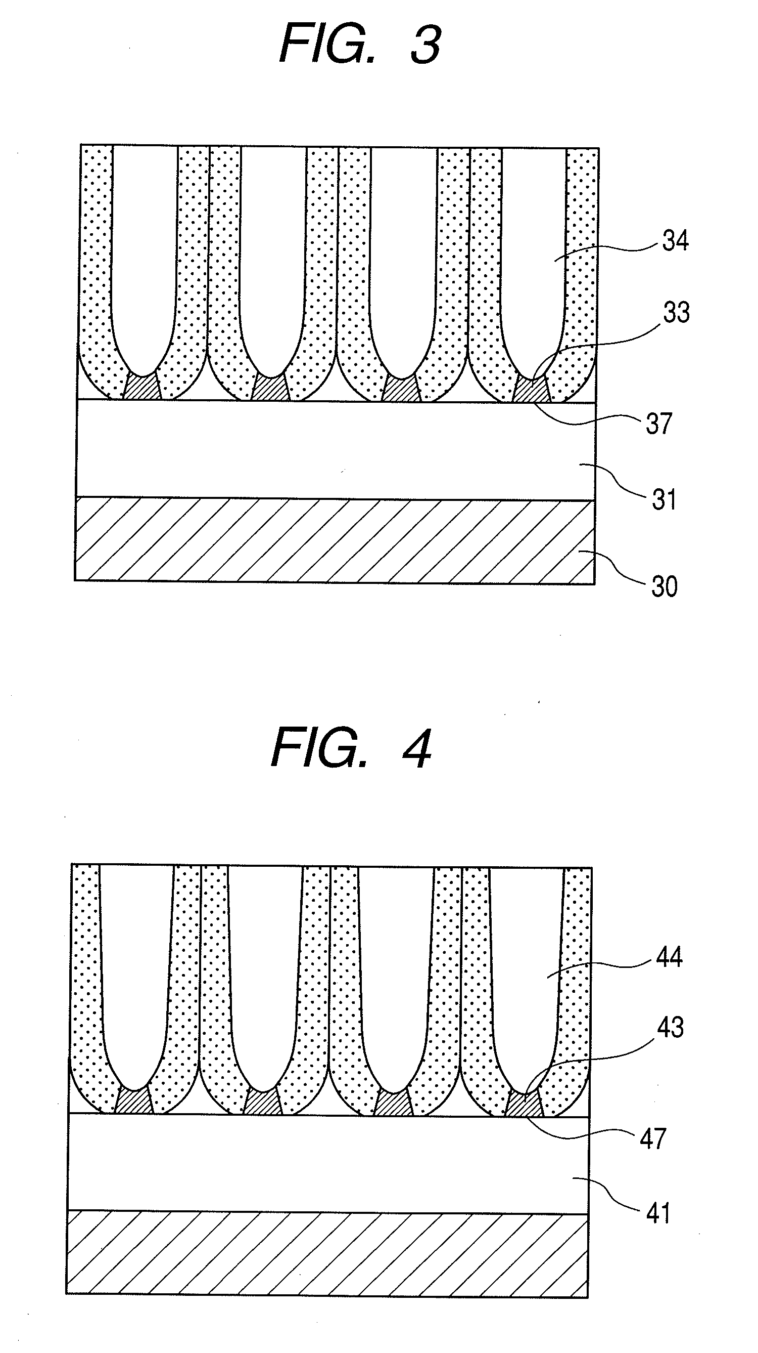
[0092]A Ti film of 5-nm thick, a Nb film of 20-nm thick as an underlying metal layer, and an AlHf layer of 35-nm thick are formed, on a Si substrate successively by sputtering. In this Example, in formation of the AlHf film, the ratio of Hf to Al is varied from 12 atom % to 5 atom % based on Al from the substrate side toward the surface side. On the AlHf surface, small dents are formed in a square array at dent intervals of 25 nm as the anodization initiation points by an FIB process. The surface AlHf layer is anodized in an aqueous 1.0-mol / L sulfuric acid solution at a bath temperature of 3° C. at an anodization voltage of 10 V. The resulting porous film layer is wet-etched for pore-widening in an aqueous 5 wt % phosphoric acid solution at a bath temperature of 20° C. The pore diameter is found to be increased from the substrate side toward the surface side by observation by FE-SEM as illustrated in FIG. 4.
[0093]The workpiece is further anodized in an aqueous 0.15-mol / L ammonium bo...
PUM
| Property | Measurement | Unit |
|---|---|---|
| temperature | aaaaa | aaaaa |
| temperature | aaaaa | aaaaa |
| temperature | aaaaa | aaaaa |
Abstract
Description
Claims
Application Information


