Semiconductor substrate for solar cell, method for manufacturing the same, and solar cell

a technology of semiconductor substrate and solar cell, which is applied in the direction of semiconductor/solid-state device manufacturing, semiconductor devices, electrical equipment, etc., can solve the problems of inability to obtain sufficient texture structure as obtained in single-crystalline silicon, crystal orientation, etc., and achieve excellent photoelectric conversion efficiency, power output, and the effect of excellent semiconductor substra

Inactive Publication Date: 2009-02-12
SHARP KK
View PDF6 Cites 14 Cited by
  • Summary
  • Abstract
  • Description
  • Claims
  • Application Information

AI Technical Summary

Benefits of technology

[0038]According to the present invention, provided can be a semiconductor substrate which has an in-plane distribution of low light reflectivities and small light reflectivities and is useful for a solar cell, and a method for manufacturing the same. In the solar cell manufactured by use of the semiconductor substrate for solar cell of the present invention, the photoelectric conversion efficiency is made better by 0.5 to 0.9 point and the power output is made better by 2 to 10% than in the solar cell manufactured by use of the semiconductor substrate manufactured by alkali etching method or the isotropic texturing method, which is a conventional method.
[0039]When the semiconductor substrate for solar cell of the present invention is a polycrystalline silicon substrate, the surface thereof exhibits a homogenous surface color similar to that of the single crystalline silicon substrate subjected to a conventional treatment. Thus, this is excellent as a semiconductor substrate for a solar cell.

Problems solved by technology

Thus, according to this technique, a sufficient texture structure as obtained in single crystalline silicon cannot be obtained in polycrystalline silicon having, in its faces, various crystal orientations.

Method used


Image

  • Semiconductor substrate for solar cell, method for manufacturing the same, and solar cell
  • Semiconductor substrate for solar cell, method for manufacturing the same, and solar cell
  • Semiconductor substrate for solar cell, method for manufacturing the same, and solar cell

Examples


example 1

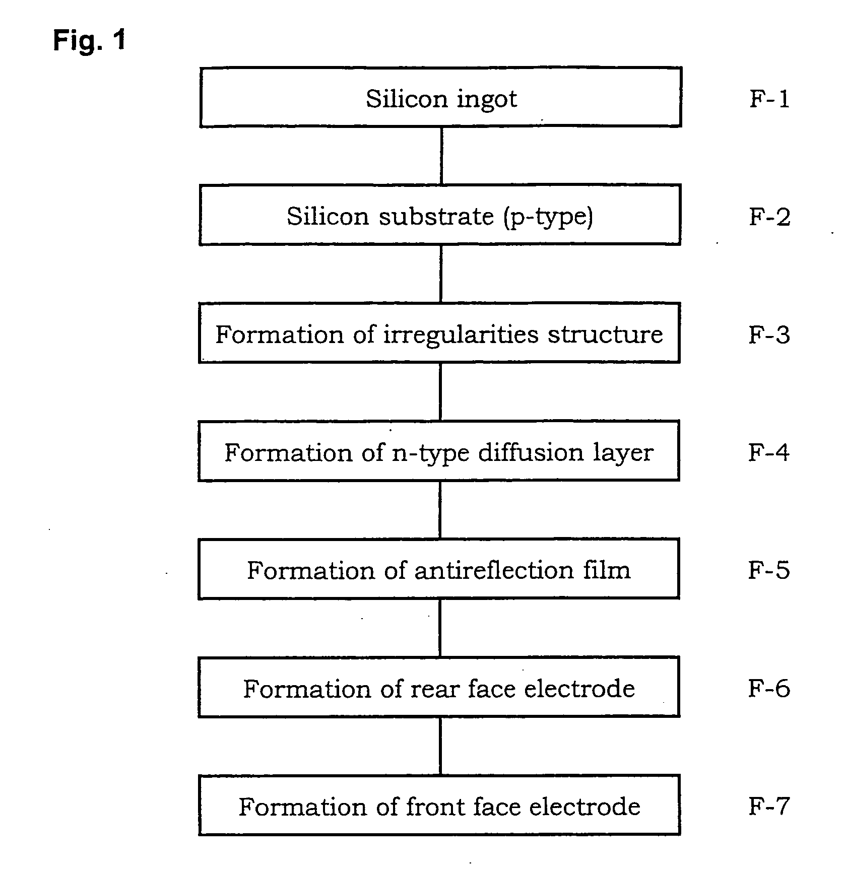
[0119]A p-type polycrystalline silicon ingot, having a resistivity of 1.2 to 1.8 Ωcm and cast by a casting method, was cut into a square pole 100 mm square with a band saw. The resultant square pole was sliced into a thickness of 300 μm with a wire saw to obtain 200 polycrystalline silicon substrates. Whenever the pole was cut into four out of the 200 polycrystalline silicon substrates, the four substrates were successively separated into 4 groups. Thus, group A, groups B, group C and group Z were obtained, in each of which the number of the substrates was 50.

[0120]The polycrystalline silicon substrates of the respective obtained groups were washed by the RCA method.

[0121]At room temperature, the polycrystalline silicon substrates of groups A and B were each immersed in a solution wherein a 60% nitric acid solution and a 50% hydrofluoric acid solution were mixed at 3 / 1 for 1 minute, so as to be etched into a depth of about 10 μm, thereby removing a damaged layer generated by the sli...

example 2

[0138]In the same way as in Example 1, 250 polycrystalline silicon substrates were obtained. Whenever five out of the 250 polycrystalline silicon substrates was cut off, the five substrates were successively separated into 5 groups. Thus, group A, group D, group E, group F and group Z were obtained, in each of which the number of the substrates was 50. The polycrystalline silicon substrates of the resultant respective groups were washed by the RCA method.

[0139]Thereafter, in the same way as in Example 1, at room temperature the polycrystalline silicon substrates of groups A, D, E and F were each immersed in a solution wherein a 60% nitric acid solution and a 50% hydrofluoric acid solution were mixed at 3 / 1 for 1 minute, so as to be etched into a depth of about 10 μm, thereby removing a damaged layer generated by the slicing.

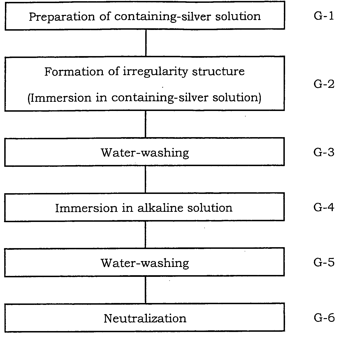
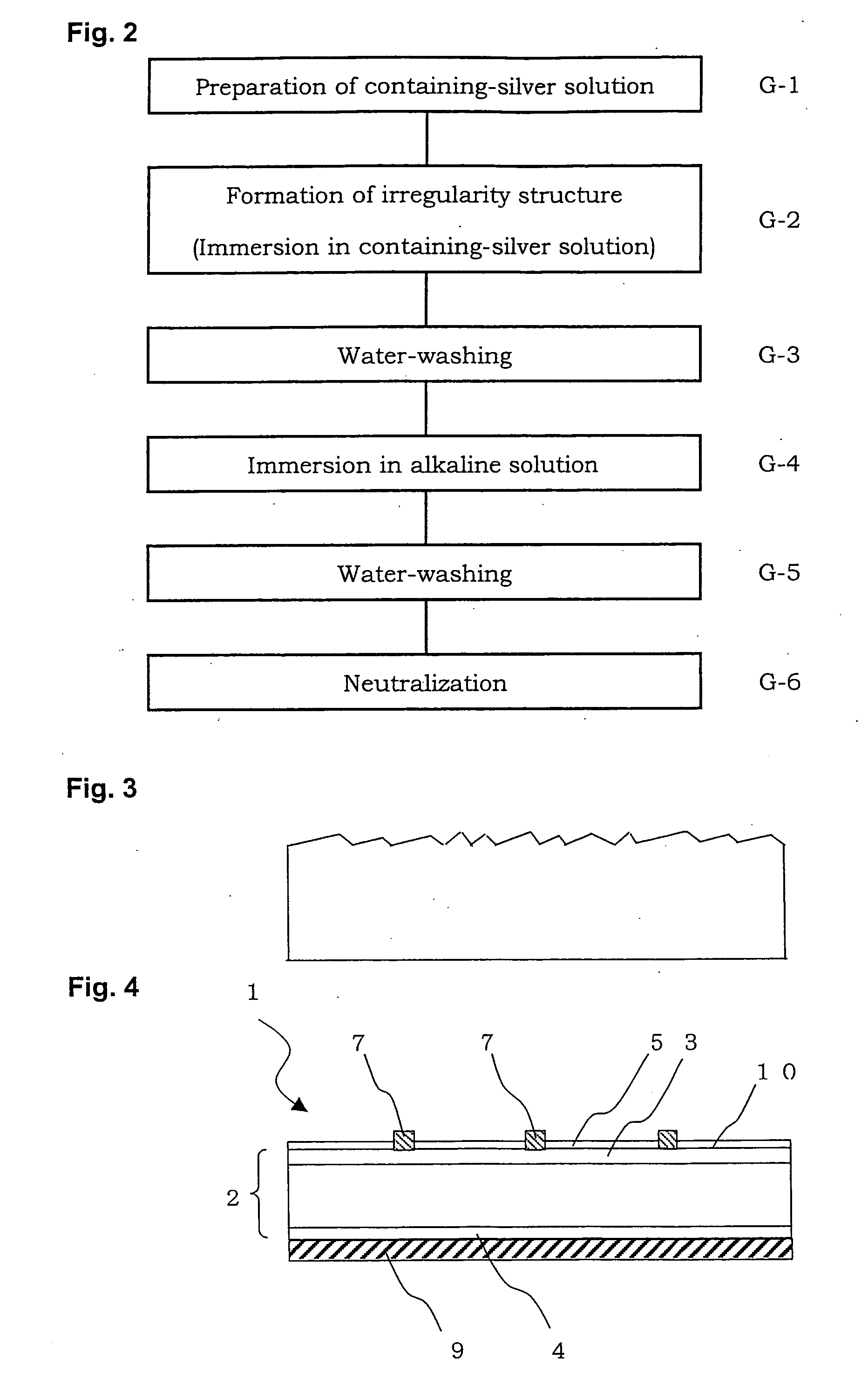
[0140]Into a mixed solution of 2L of a 50% hydrofluoric acid solution and 60 mL of a 60% nitric acid solution was dissolved 5 g of pure silver powder to obtain a...


PUM


Abstract

A semiconductor substrate for a solar cell, comprising the semiconductor substrate having a surface which constitutes a light incident face of the solar cell and having a surface irregularities structure, wherein the surface has an surface area from 1.2 to 2.2 times that of an imaginary smooth face and the standard deviation of the heights of the irregularities is 1.0 μm or less.

Description

TECHNICAL FIELD[0001]The present invention relates to a semiconductor substrate for a solar cell, a method for manufacturing the same, and a solar cell. More specifically, the present invention relates to a semiconductor substrate for a solar cell having a reduced light reflectivity, a method for manufacturing the same at low cost, and a high-performance solar cell manufactured by use of the method.BACKGROUND ART[0002]Solar cells wherein pn junctions are formed in a semiconductor substrate, such as a single crystalline silicon substrate or a polycrystalline silicon substrate, are main current solar cell products.[0003]FIG. 4 is a schematic cross-sectional view of a polycrystalline silicon solar cell. This polycrystalline silicon solar cell 1 is manufactured, for example, as follows. First, a silicon ingot manufactured by a casting method is sliced by a multi-wire method, so as to obtain a p-type silicon substrate 2. Next, at least the whole of the light-receiving face of the p-type ...

Claims


Application Information

Patent Timeline
Patent Type & Authority Applications(United States)
IPC IPC(8): H01L31/0368H01L31/18H01L21/306H01L31/0236H01L31/04
CPCH01L31/02363Y02E10/50
Inventor KOMATSU, YUJIFUKUMURA, HIROYUKITAKABA, YOSHIROHOZAKI, RYOHNUNOI, TOHRU
Owner SHARP KK
Why Eureka
Try Eureka