
White LED device comprising dual-mold and manufacturing method for the same

a technology of led devices and manufacturing methods, applied in the direction of discharge tubes/lamp details, discharge tubes luminescnet screens, electric discharge lamps, etc., can solve the problems of difficult mass production of white led devices with high luminance and spectral uniformity, and the process of manufacturing the devices is complicated, so as to improve improve the effect of color reappearance, and improve the effect of color rendering and spectral distribution

Inactive Publication Date: 2009-02-12
ST&I
View PDF9 Cites 57 Cited by
  • Summary
  • Abstract
  • Description
  • Claims
  • Application Information

AI Technical Summary

Benefits of technology

[0029]The inventive white LED device creates white light by mixing blue, red, and green light. Therefore, the white LED device has improved color rendering and spectral distribution to provide a good color temperature and emit white light close to natural white light. Moreover, the inventive white LED device has excellent color reappearance as well as high luminance and efficiency.
[0030]Meanwhile, the inventive white LED device manufacturing method has an advantage in that conventional manufacturing methods are all applicable. That is, the white LED device can be manufactured using a transfer-molding technique or the like, as well as a potting technique, and a screen pattern metal mask technique. Specifically, if a two-step curing process is used, the phosphor can be uniformly dispersed in the transparent epoxy resin. Therefore, the white LED device can be manufactured to have high luminance and excellent reproducibility.
[0031]The inventive white LED device having the dual mold has numerous applications such as in a display emitting white light, in automobile control displays, home appliances, electronic devices such as portable phones, in liquid crystal displays, etc. The inventive white LED device is applicable to electronic devices currently employing LEDs or fluorescent lamps.

Problems solved by technology

As a result, the conventional white LED device has a drawback in that since the emitted white light is weaker in intensity in the red wavelength region than in the yellow wavelength region, it is not recognized as being very close to natural white light.
Further, the conventional white LED device has a disadvantage in that since a spectrum of the emitted white light varies widely according to the intensity of the yellow wavelength region, it is difficult to mass produce the white LED device with high luminance and spectral uniformity.
Additionally, since the spectrum of white light output by the conventional white LED device has the single peak in the yellow wavelength region, a process for manufacturing the device is complicated.

Method used


Image

  • White LED device comprising dual-mold and manufacturing method for the same
  • White LED device comprising dual-mold and manufacturing method for the same
  • White LED device comprising dual-mold and manufacturing method for the same

Examples


embodiments

[0059]FIG. 11 is a flowchart illustrating a method of manufacturing a white LED device having dual molds according to a second embodiment of the present invention.

[0060]The white LED device of FIG. 6 is manufactured using the manufacturing process of FIG. 11, which is characterized by use of a transfer-molding technique. The transfer-molding technique will be described only briefly because it is widely known in the field of LED chip packaging.

[0061]Referring to FIG. 11, after a chip adhering process is performed to mount the blue LED chip 114 on the LED chip mounting member 124 as in the first embodiment (S410), the wire bonding process (S118) is performed if needed (S420). Also, the transfer-molding technique is used to form the first mold 110a and 112 (S430). The transfer-molding technique can be performed using a first base resin tablet having the first phosphor, for example, the red phosphor 112, mixed in the epoxy mold compound (EMC). The first mold 110a and 112 is formed to ha...


PUM


Abstract

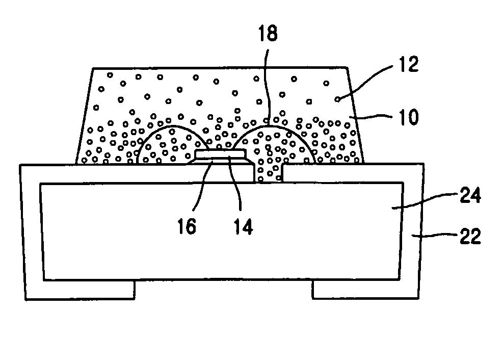
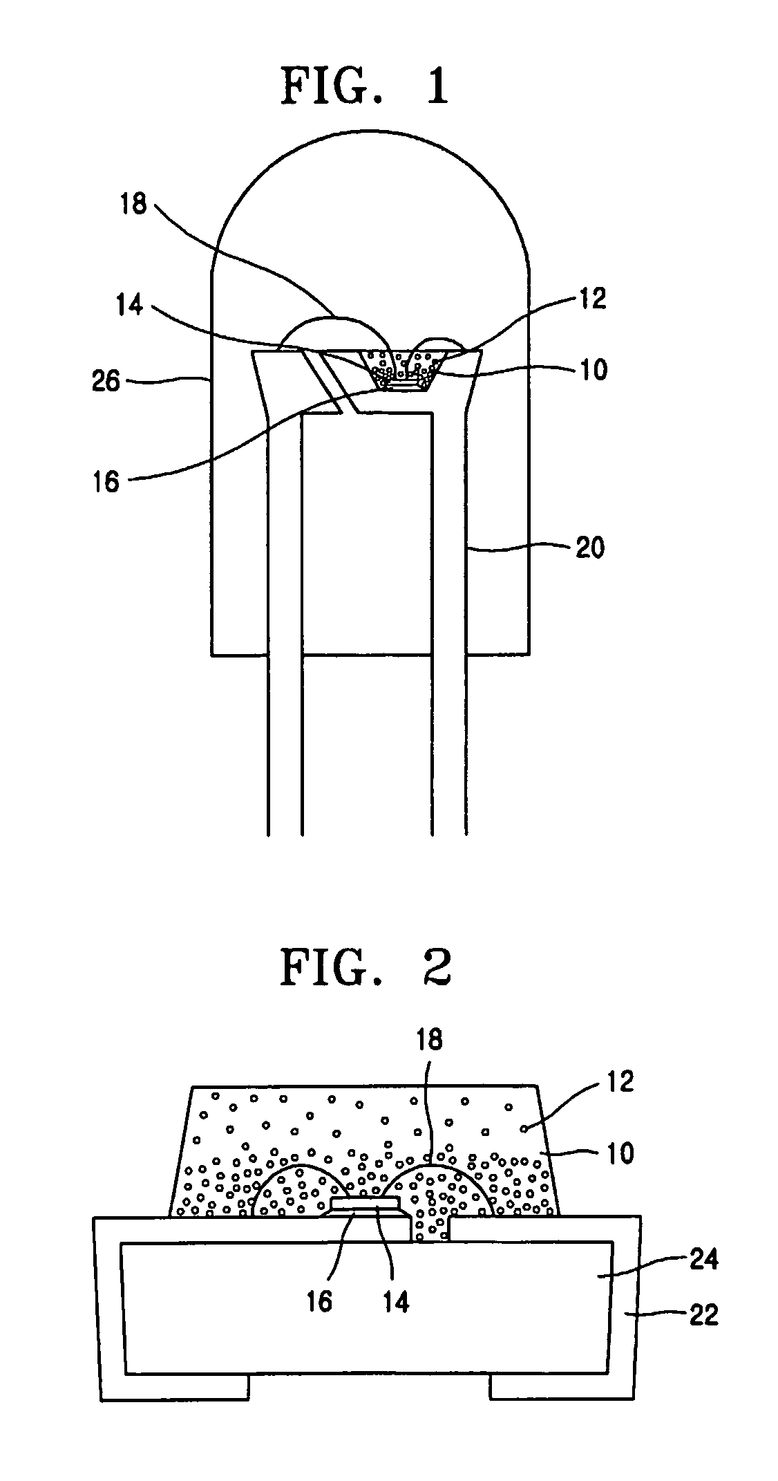
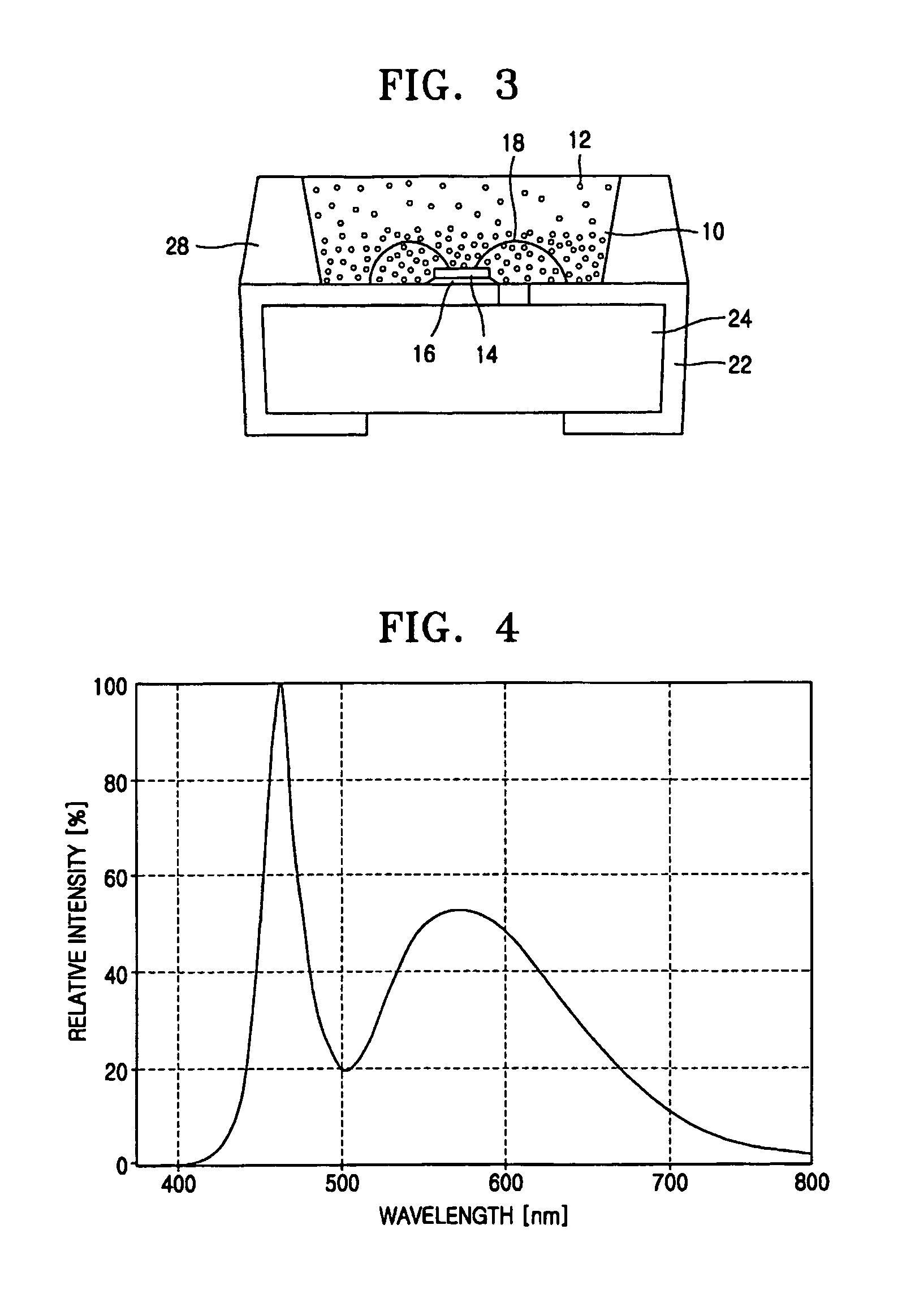
A conventional high-luminance white light emitting diode (LED) device has the disadvantage of it being difficult to achieve high luminance and excellent and uniform quality since emitted light is weaker in the red wavelength region than at yellow wavelengths. The present invention provides a high-luminance white LED device with improved color rendering and spectrum distribution, and a method of manufacturing the same. The white LED device according to one embodiment of the present invention is characterized by dual molds. The white LED device includes: an LED chip mounting member for mounting an LED chip; at least one blue LED chip or ultraviolet LED chip mounted on the LED chip mounting member; a first mold having a transparent epoxy resin and a first phosphor and sealing the blue or ultraviolet LED chip, the first phosphor dispersed in the transparent epoxy resin to convert light emitted from the blue or ultraviolet LED chip into first light having a first wavelength; and a second mold having a transparent epoxy resin and a second phosphor and formed on the first mold, the second phosphor dispersed in the transparent epoxy resin to convert light emitted from the blue or ultraviolet LED chip into second light having a second wavelength, the second light being white light obtained by combination of the emitted light with the first light. The white LED device having the dual molds can be a lamp-type LED device, an injection-molded housing package-type LED device, or a transfer-molded chip-type LED device.

Description

TECHNICAL FIELD[0001]The present invention relates to a white light emitting diode (LED) device and a method of manufacturing the same, and more particularly, to a white LED device using a blue or ultraviolet LED chip, and a method of manufacturing the same.BACKGROUND ART[0002]An LED device is a kind of semiconductor device for converting electrical energy into light energy using a characteristic of compound semiconductors. LED devices come in blue, white, and seven-color varieties, and their applications are continuously increasing. Among the three varieties, white LED devices are currently used in high-luminance flashlights, in a backlight of a liquid crystal display (LCD) of portable electronic devices (portable phones, camcorders, digital cameras and personal digital assistants (PDAs)), in electronic display boards, in indicators and switches, and in display lights and traffic lights, etc.[0003]The white LED device converts a part of light emitted from an LED chip into light hav...

Claims


Application Information

Patent Timeline
Patent Type & Authority Applications(United States)
IPC IPC(8): H01L33/00H01J1/62H01L33/50H01L33/54H01L33/56
CPCH01L33/56H01L33/504H01L2224/48247H01L2224/48091H01L2224/73265H01L2924/181H01L2924/00014H01L2924/00012
Inventor PARK, JUN-KYUYOO, JAE-HYOUNG
Owner ST&I
Learn More