Ceramic electronic component and method for manufacturing the same

a technology of ceramic electronic components and ceramic components, which is applied in the direction of fixed capacitor details, stacked capacitors, fixed capacitors, etc., can solve the problems of inability to provide sufficient stress reduction, and cracking of laminated ceramic capacitors, so as to prevent the oxidation of the surface of electrically conductive resin layers , the effect of reducing the absolute value of silver and reducing the migration of silver

Active Publication Date: 2009-02-12
MURATA MFG CO LTD
View PDF1 Cites 34 Cited by
  • Summary
  • Abstract
  • Description
  • Claims
  • Application Information

AI Technical Summary

Benefits of technology

[0025]In preferred embodiments of the present invention, if the silver-coated copper powder is used as the electrically conductive filler included in the electrically conductive resin layer, oxidation of the surface of the electrically conductive resin layer is prevented. In addition, the absolute value of silver is reduced and, thereby, the migration of silver can be reduced. When the phenol resin is used as the thermosetting resin included in the electrically conductive resin layer, a reducing effect can be exerted during heat-curing and, thereby, oxidation of a portion of the sur

Problems solved by technology

Consequently, there is a problem in that the end of the terminal electrode is vulnerable to a tensile stress.
If the electrically conductive resin layer is peeled during mounting of the laminated ceramic capacitor, as described above, when a large stress i

Method used


Image

  • Ceramic electronic component and method for manufacturing the same
  • Ceramic electronic component and method for manufacturing the same
  • Ceramic electronic component and method for manufacturing the same

Examples


first preferred embodiment

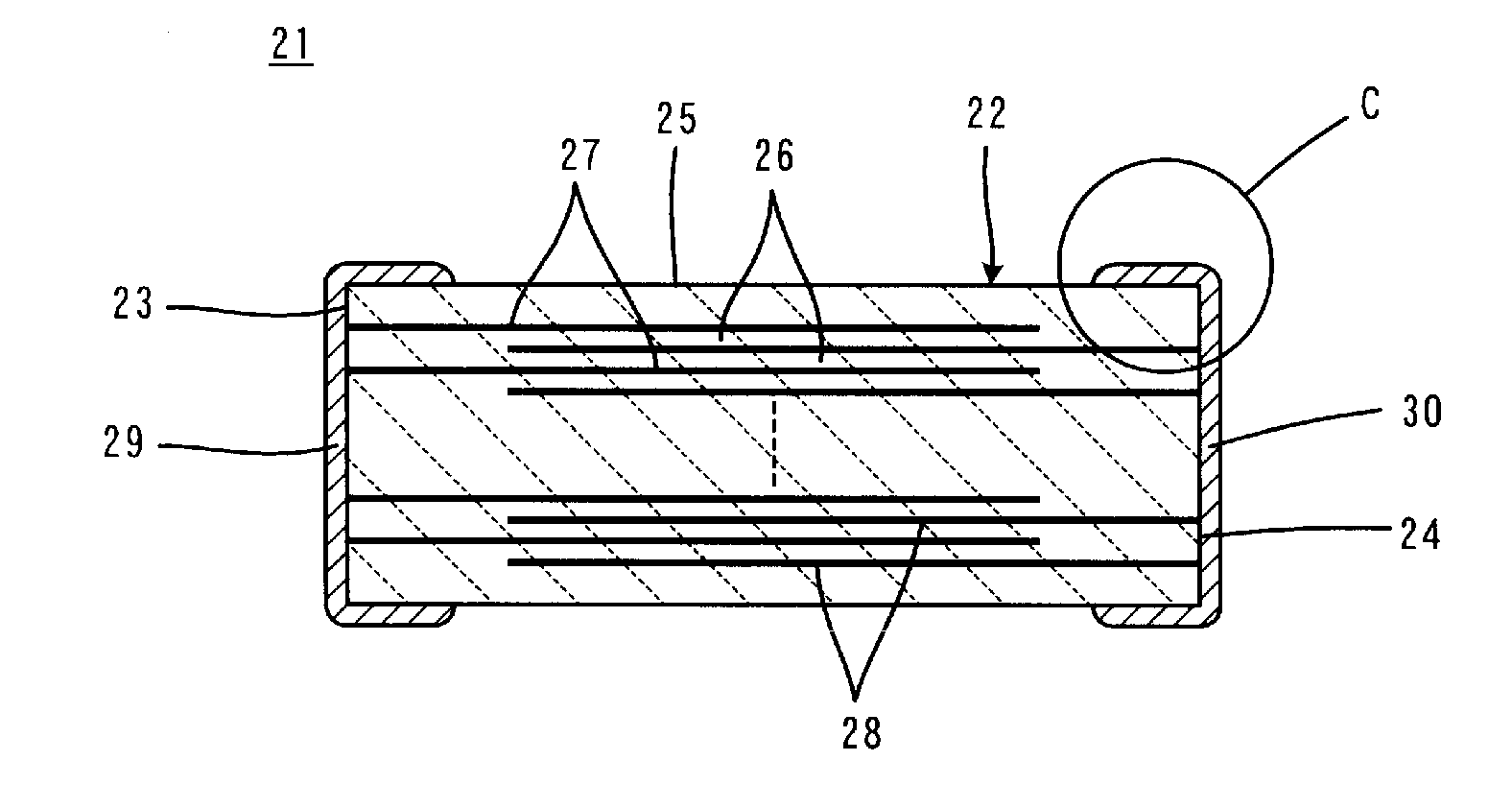
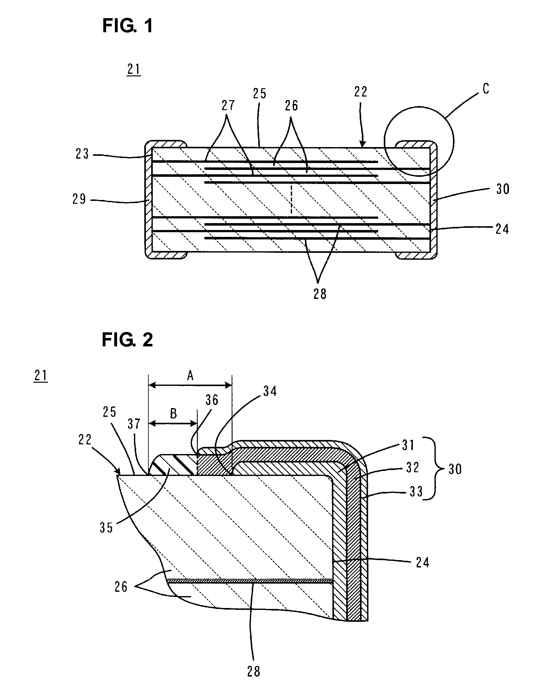
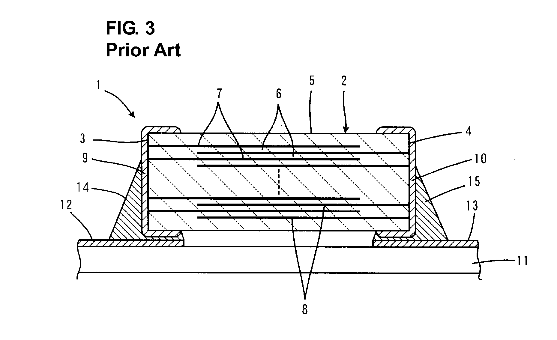
[0033]FIG. 1 is a sectional view showing a laminated ceramic capacitor 21 according to a preferred embodiment of the present invention. FIG. 2 is a sectional view of a magnified portion C shown in FIG. 1. The laminated ceramic capacitor 21 shown in FIGS. 1 and 2 has substantially the same structure as the structure of the laminated ceramic capacitor 1 shown in FIG. 3 except for the structure of the terminal electrode.

[0034]The laminated ceramic capacitor 21 includes an electronic component main body 22 made of ceramic. The electronic component main body 22 includes two end opposed surfaces 23 and 24 and a side surface 25 extending between the opposed end surfaces 23 and 24. Furthermore, the electronic component main body 22 includes a plurality of laminated dielectric ceramic layers 26 and internal electrodes 27 and 28 disposed along specific interfaces between the dielectric ceramic layers 26.

[0035]The laminated ceramic capacitor 21 includes terminal electrodes 29 and 30 arranged t...


PUM

PropertyMeasurementUnit
Lengthaaaaaaaaaa
Pressureaaaaaaaaaa
Lengthaaaaaaaaaa

Abstract

In a ceramic electronic component, an electrically conductive resin layer is arranged to cover a thick film layer and to extend beyond the end of the thick film layer by at least about 100 μm and a plating layer is arranged to cover the electrically conductive resin layer except a region having a dimension of at least about 50 μm and extending along the end of the electrically conductive resin layer. Consequently, the concentration of the stress is reduced.

Description

BACKGROUND OF THE INVENTION[0001]1. Field of the Invention[0002]The present invention relates to a ceramic electronic component and a method for manufacturing the same. In particular, the present invention relates to the structure of a terminal electrode included in a ceramic electronic component and a method for manufacturing the same. 2. Description of the Related Art[0003]Examples of known ceramic electronic components include laminated ceramic electronic components, e.g., laminated ceramic capacitors. FIG. 3 is a sectional view showing a conventional laminated ceramic capacitor 1.[0004]The laminated ceramic capacitor 1 includes an electronic component main body 2 made of ceramic. The electronic component main body 2 has two opposed end surfaces 3 and 4 and a side surface 5 extending between the end surfaces 3 and 4. The electronic component main body 2 includes a plurality of laminated dielectric ceramic layers 6 and internal electrodes 7 and 8 disposed along interfaces between ...

Claims


Application Information

Patent Timeline
IPC IPC(8): H01G4/12C25D5/02H01G4/232H01G4/252H01G4/30
CPCH01G4/2325H01G4/252H01G13/006H01G4/30H01G4/12
Inventor KAYATANI, TAKAYUKI
Owner MURATA MFG CO LTD
Why Eureka
Try Eureka