Method for fabricating semiconductor integrated circuit

a technology of integrated circuit and semiconductor, which is applied in the direction of semiconductor devices, semiconductor/solid-state device details, electrical equipment, etc., can solve the problems of difficult deposit of conductive film for wiring in through-hole, cvd-tin film embedded in through-hole, and difficult to corrode al (aluminum) wiring, etc., to achieve the effect of reducing film making temperature, reducing copper corrosion, and reducing the difficulty of corroding particularly easily

Inactive Publication Date: 2005-02-08
LONGITUDE SEMICON S A R L
View PDF22 Cites 12 Cited by
  • Summary
  • Abstract
  • Description
  • Claims
  • Application Information

AI Technical Summary

Benefits of technology

In the semiconductor device using a copper wiring layer, which is corroded particularly easily, the copper corrosion can be mitigated by providing a trap film such as of tantalum or tantalum nitride between the titanium nitride film containing a halogen element and the copper wiring layer.
When the titanium nitride film formed by the CVD method is used for one of the electrodes of the capacitor, the trap film such as a titanium film made by sputtering is formed over this titanium nitride film. Conventionally, polysilicon has primarily been used for the electrodes of capacitors. Polysilicon films must be formed at a high temperature of about 650° C. The film making temperature can be reduced by the use a titanium nitride film formed by a CVD method using a source gas containing halogen as a constitutional element. The film making temperature of the titanium nitride film by the CVD method is 400° C. to 600° C. The relation between chlorine concentration in the titanium nitride film and the film making temperature when titanium tetrachloride is used as a source gas is shown in FIG. 46. As shown in this graph, lower film making temperature results in higher chlorine concentration in the titanium nitride film. Particularly when the film is made at temperatures below 500° C., the extent to which the wiring layer around the storing capacitor is corroded increases. Thus, the effect to prevent corrosion of the wiring layer becomes great if the trap film of this invention is provided particularly when the titanium nitride film is formed at temperature below 500° C. Not only when a titanium nitride film containing halogen is formed as the storage electrode but also when a titanium nitride film is formed after an aluminum wiring layer has been formed, it is preferable that the film making temperature be below 500° C. Forming the film at low temperatures increases the content of halogen in the titanium nitride film.
The corrosion of the conductive film can also be prevented by forming a titanium nitride film using a source gas containing halogen as a constitutional element and then annealing it in an inert gas such as nitrogen gas or rare gas. That is, annealing can remove halogen from the titanium nitride film. The annealing is performed at a temperature of 400° C. to 800° C., preferably at a temperature higher than that of the process in which a TiN film is formed by the CVD method. If annealing is done in the same apparatus as the film making apparatus without exposing the titanium nitride film to the atmosphere immediately after the titanium nitride film is formed, the oxidation of the surface of the titanium nitride film can be prevented. The cleaning process may be omitted. If the cleaning process is performed, it may be done either before or after the annealing, preferably after annealing. The use of warm water at 40° C. or higher during cleaning is most effective in removing chlorine.
If water enters the titanium nitride film during a certain processing, chlorine becomes more freely movable in the device and thus the amount of chlorine moving toward the wiring layer increases, rendering the wiring layer more likely to be corroded. It is considered that the reason is because chlorine in the titanium nitride film, when contacting water, is ionized and become more freely movable seeking species to bond to. To prevent ingress of water into the titanium nitride film, the titanium nitride film is formed by using a source gas containing halogen as a constitutional element, followed by the forming of a high-density plasma CVD insulating film that has a high water blocking effect. The refractive index of the insulating film is above 1.46, and the insulating film includes Si rich. The processes during which water can enter the film include the cleaning process after dry etching and the inorganic spin-on-glass (SOG) film forming process. The inorganic SOG film forming process involves applying an inorganic SOG film and then performing a steam-baking whereby the film is baked in water steam. Thus, by forming a high-density plasma CVD insulating film under the inorganic SOG film, the corrosion of the wiring layer can be reduced. An organic SOG film may be formed instead of the high-density plasma CVD film because the organic SOG film also has a water blocking capability, though not as high as that of the high-density plasma CVD insulating film.

Problems solved by technology

When the aspect ratio of a through-hole (depth / diameter of the through-hole) for connecting upper- and lower-layer wirings formed on a semiconductor substrate is increased as an LSI is further refined and more densely integrated, it is difficult to deposit a conductive film for wiring in the through-hole.
However, because a TiN film formed by using a source gas containing a halogen element contains a halogen element such as chlorine produced due to decomposition of the source gas, there is a problem that the Al (aluminum) wiring formed on a through-hole in which a CVD-TiN film is embedded would be corroded because the halogen element reacts with Al.
Further, the tungsten film has a poor adhesion to the underlying film and is easily peeled.

Method used


Image

  • Method for fabricating semiconductor integrated circuit
  • Method for fabricating semiconductor integrated circuit
  • Method for fabricating semiconductor integrated circuit

Examples


embodiment 1

The preferred embodiments of the present invention are described below in detail by referring to the accompanying drawings. Similar elements are provided with the same symbol and their repetitive description is omitted.

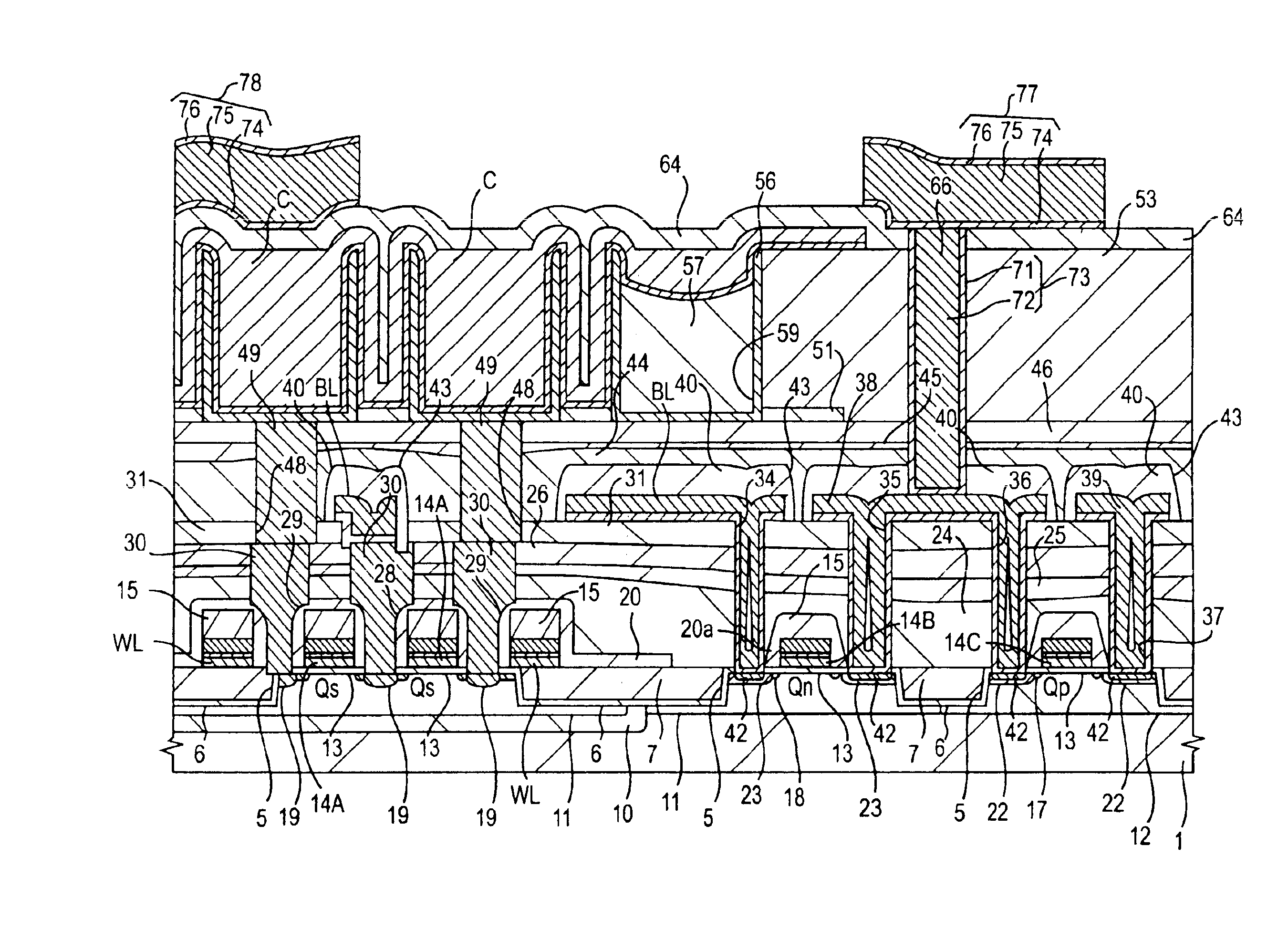
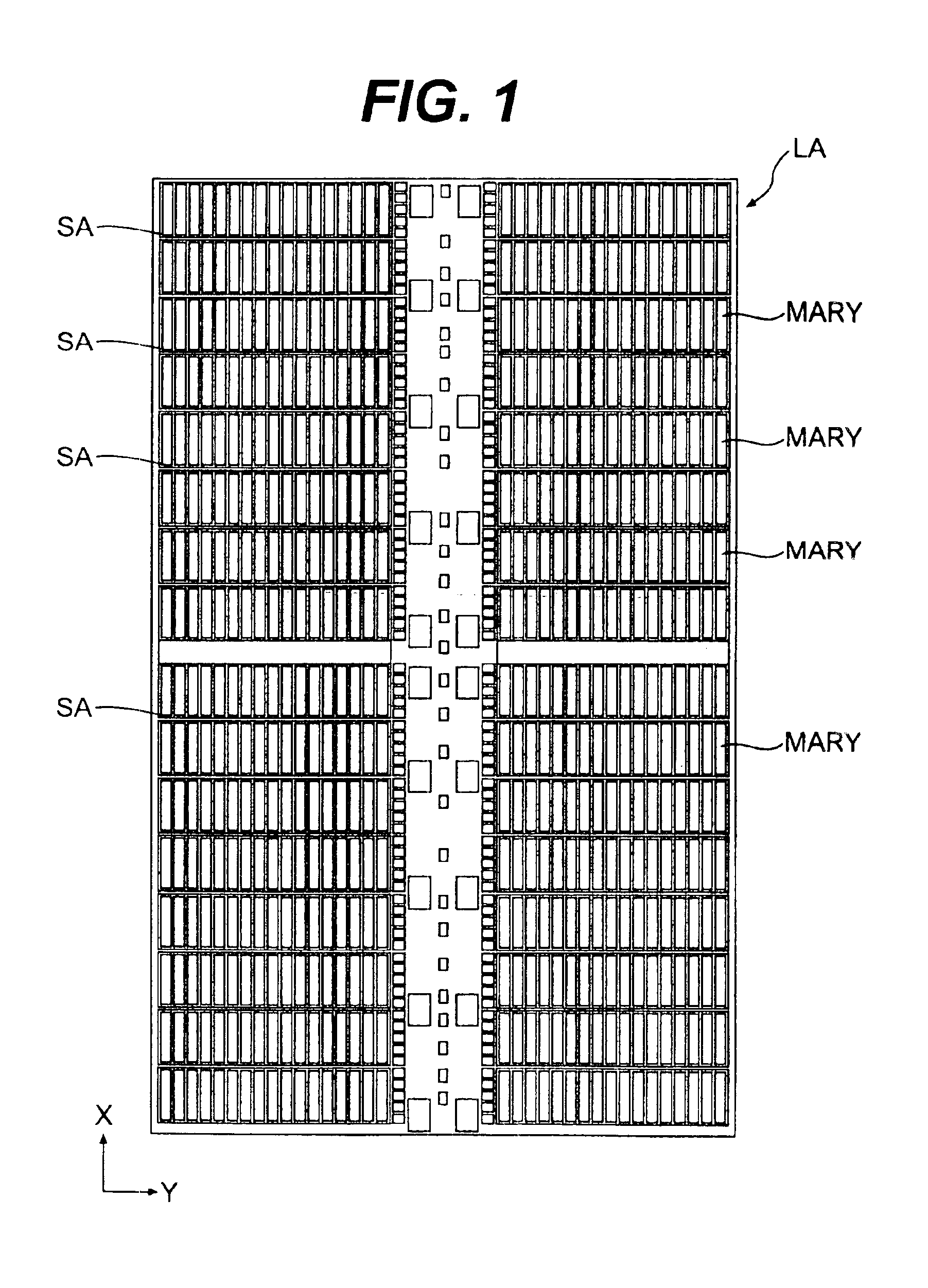
FIG. 1 is a top view of a semiconductor chip on which the DRAM of this embodiment is formed. As shown in FIG. 1, a lot of memory arrays MARY are arranged on the principal plane of a semiconductor chip 1A made of single-crystal silicon like a matrix along the X direction (major-side direction of the semiconductor chip 1A) and the Y direction (minor-side direction of the semiconductor chip 1A). A sense amplifier SA is set between the memory arrays MARY adjacent to each other along X direction. Control circuits such as a word driver WD and a data-line selection circuit and an input / output circuit and a bonding pad are arranged at the central portion of the principal plane of the semiconductor chip 1A.

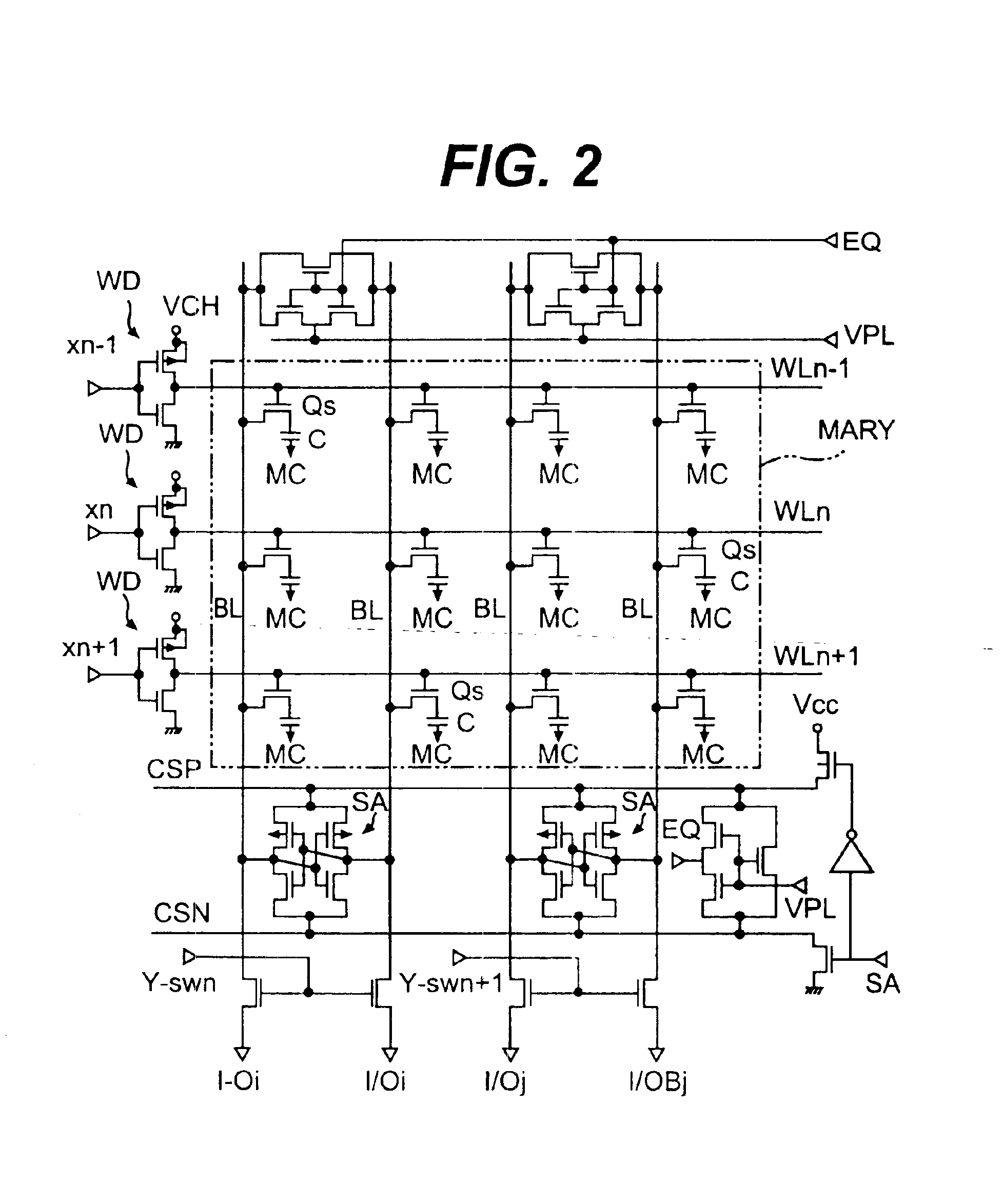
FIG. 2 is an equivalent circuit diagram of the DRAM. As shown in FIG. 2...

embodiment 2

This embodiment is an example where the device uses a titanium nitride film containing a halogen element as one of electrodes of a storing capacitor section.

FIG. 47 shows a cross section of the capacitor. One electrode 101 of the capacitor and a capacitor insulating film 102 of tantalum oxide are formed in the same manner as the embodiment 1. Although the capacitor insulating film of this embodiment uses a tantalum oxide film, it may use a ferrodielectric film such as of BST and PZT. Then, using a gas mixture of titanium tetrachloride and ammonia as a source gas, a titanium nitride film 103 is formed to a thickness of 50-100 nm by the chemical vapor deposition method. This titanium nitride film is formed at about 500° C. and contains about 4% of chlorine. The upper electrode has an advantage that when it is formed of titanium nitride instead of conventionally used polysilicon, it can be formed at a lower temperature. After this, a titanium film 104 is formed to a thickness of about ...

embodiment 3

This embodiment is an example in which a titanium nitride film 105 is formed by the sputtering method over the sputtered titanium film 104 of the Embodiment 2, and will be described referring to FIG. 48. The process up to the formation of the capacitor insulating film of tantalum oxide is similar to those of Embodiment 1 and 2. After this, a titanium film 104 was sputtered to a thickness of 40 nm and a titanium nitride film 105 formed to 60 nm by chemical conversion sputter using the flow of nitrogen gas. The use of a multilayer film of the titanium film 104 formed by sputtering and the titanium nitride film 105 formed by sputtering as the chlorine trapping layer enabled almost complete trapping of chlorine and enhanced the effect to prevent corrosion of the wiring layer around the capacitor.

While, in this embodiment, the titanium film of 104 to 40 nm thickness is formed by sputtering and the titanium nitride film of 105 to 60 nm thickness is formed, the thickness of the titanium fi...


PUM


Abstract

The semiconductor device is formed according to the following steps. A TiN film 71 and a W film 72 are deposited on a silicon oxide film 64 including the inside of a via-hole 66 by the CVD method and thereafter, the W film 72 and TiN film 71 on the silicon oxide film 64 are etched back to leave only the inside of the via-hole 66 and form a plug 73. Then, a TiN film 74, Al-alloy film 75, and Ti film 76 are deposited on the silicon oxide film 64 including the surface of the plug 73 by the sputtering method and thereafter, the Ti film 76, Al-alloy film 75, and TiN film 74 are patterned to form second-layer wirings 77 and 78.

Description

BACKGROUND OF THE INVENTIONThe present invention relates to a semiconductor integrated circuit device and a technique of fabricating a semiconductor integrated circuit device, and more particularly to measures for preventing corrosion of an upper-layer wiring when a TiN film is formed inside a through-hole for connecting upper- and lower-layer wiring formed over a semiconductor substrate and over an upper electrode of a capacitor insulating film, by a chemical vapor deposition method using a metal source containing a halogen element.When the aspect ratio of a through-hole (depth / diameter of the through-hole) for connecting upper- and lower-layer wirings formed on a semiconductor substrate is increased as an LSI is further refined and more densely integrated, it is difficult to deposit a conductive film for wiring in the through-hole. Therefore, an art for embedding a plug in a through-hole having a high aspect ratio in a plug has been used so far.As described in Japanese Patent Laid...

Claims


Application Information

Patent Timeline
Patent Type & Authority Patents(United States)
IPC IPC(8): H01L21/70H01L23/522H01L23/52H01L21/8242
CPCH01L23/5226H01L27/10852H01L2924/0002H01L2924/00H10B12/033H01L27/10
Inventor NAKAMURA, YOSHITAKATAMARU, TSUYOSHIFUKUDA, NAOKIGOTO, HIDEKAZUASANO, ISAMUAOKI, HIDEOKAWAKITA, KEIZOYAMADA, SATORUTANAKA, KATSUHIKOSAKUMA, HIROSHIHIRASAWA, MASAYOSHI
Owner LONGITUDE SEMICON S A R L
Why Eureka
Try Eureka