
Industrialized thick GEM (Gaseous Electron Multiplier) manufacturing method

A manufacturing method and original board technology, applied in cold cathode manufacturing, electrode system manufacturing, discharge tube/lamp manufacturing, etc., can solve problems such as difficulty in increasing the size of insulating rings, inability to meet mass production, and quality assurance

Active Publication Date: 2013-09-04
INST OF HIGH ENERGY PHYSICS CHINESE ACADEMY OF SCI +1
View PDF3 Cites 12 Cited by
  • Summary
  • Abstract
  • Description
  • Claims
  • Application Information

AI Technical Summary

Problems solved by technology

This process needs to be combined with a laser lithography system with high positioning accuracy, the cost is high, and its rim can also reach 100μm
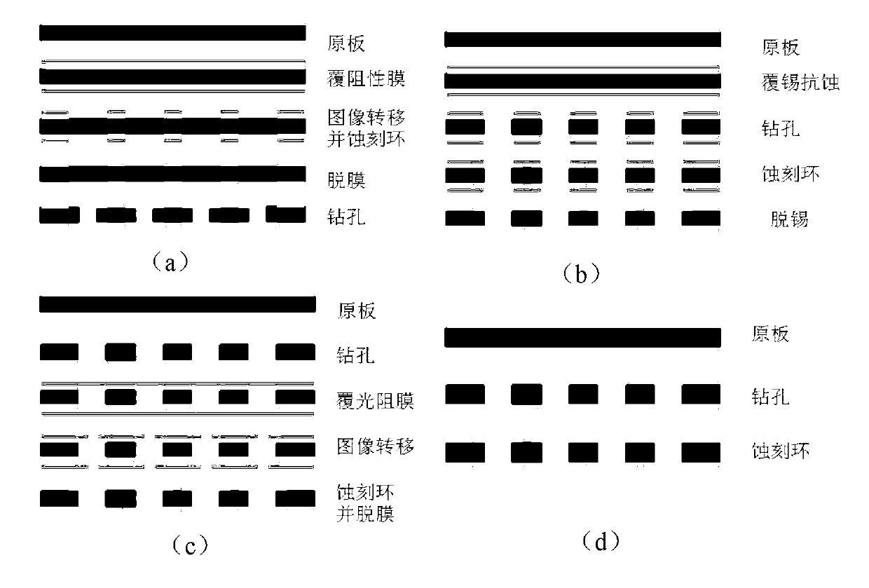
The fourth ( figure 1 d) It does not cover any protective film, and the entire plate is directly etched after mechanical drilling, so that the thickness of the copper layer will decrease with the increase of the rim size, and the control is relatively difficult
[0013] First of all, the production cost is high, and the delivery time cycle of thick GEM is uncertain, generally long, which cannot meet the requirements of mass production
[0014] Secondly, the post-processing method of self-corrosion insulating ring is adopted, which not only needs to be equipped with corresponding chemical etchant and equipment in the laboratory, but also requires manual control and operation, which is time-consuming and labor-intensive, with poor controllability and repeatability. not guaranteed
And the high-energy self-etching thick GEM basically cannot work in the mixed gas of argon and carbon dioxide
[0015] Furthermore, the insulating ring (rim) around the hole is formed through the full-page etching process, and the size of the insulating ring is difficult to increase. Generally, the size of the insulating ring is <40 μm

Method used


Image

  • Industrialized thick GEM (Gaseous Electron Multiplier) manufacturing method
  • Industrialized thick GEM (Gaseous Electron Multiplier) manufacturing method
  • Industrialized thick GEM (Gaseous Electron Multiplier) manufacturing method

Examples


Embodiment Construction

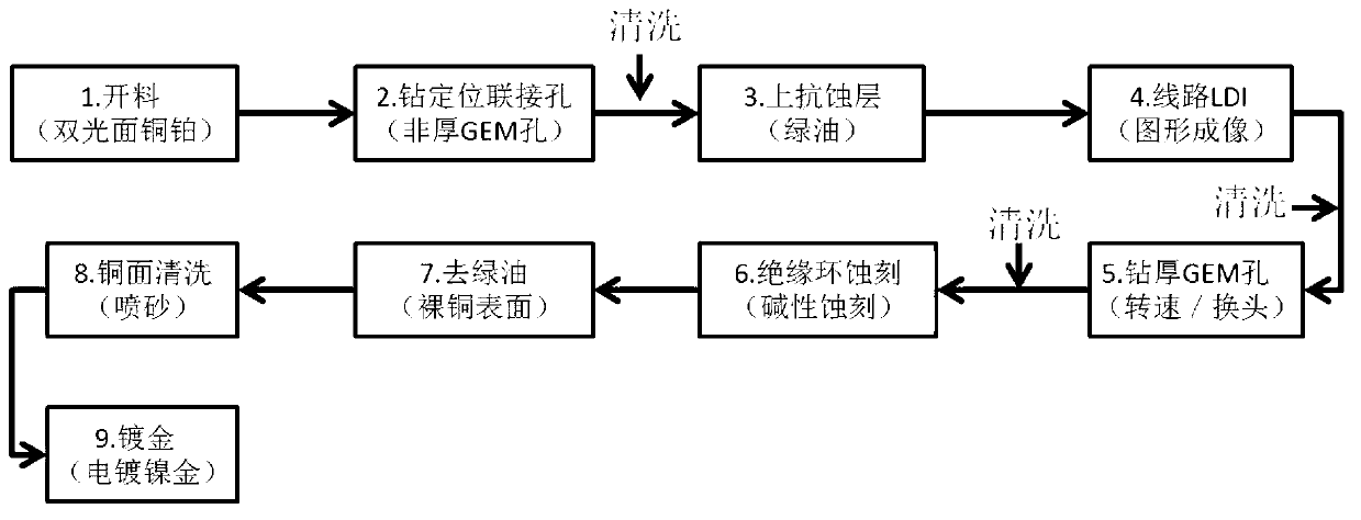
[0058] The general technical process of the present invention is as image 3 Shown, including 9 processes. Among them, it is very important to perform additional cleaning on the plate before and after process 3, and before and after process 5. The main purpose is to remove tiny particles or debris on the plate and the processing platform, which can effectively avoid defects and improve the yield. Generally, ultrasonic cleaning or air blowing can be used. The following is a detailed description of each process link:

[0059] Process 1: cutting

[0060] Whether it is from PCB processing or thick GEM production, I have never paid attention to raw materials before. During our initial process of making thick GEM, we found that thick GEM is very easy to ignite in the mixed gas of argon and carbon dioxide. Basically, it starts to ignite as soon as the signal is issued, and there is no working linear region. There are two reasons for sparking in the mixed gas of argon and carbon d...


PUM


Abstract

The invention discloses an industrialized thick GEM (Gaseous Electron Multiplier) manufacturing method, which comprises the following steps: (1) preparing positioning and connecting holes in a thick GEM original plate; (2) covering the thick GEM original plate treated by the step (1) with a corrosion resistant layer; (3) transferring the design image to the thick GEM original plate treated by the step (2); (4) preparing thick GEM holes in the thick GEM original plate treated by the step (3); (5) preparing insulating rings for all thick GEM holes; and (6) removing the corrosion resistant layer on the thick GEM original plate. The performance can be further improved by plating a gold layer on the thick GEM original plate treated by the step (6). According to the industrialized thick GEM manufacturing method, low-cost, short-period, large-area and high-yield industrialized whole assembly line batch production of the domestic thick GEM original plate is realized; the produced thick GEM has high gain and good gain stability and energy resolution, is ignition-resistant and can work in various argon-based and neon-based mixed gases.

Description

technical field [0001] The invention relates to an industrial thick GEM manufacturing method. The invention is based on common domestic PCB processing and chemical corrosion technology and equipment, and realizes the mass production of THick gaseous electron multiplier (THick gaseous electron multiplier, THGEM, thick GEM). At present, such thick GEM detectors are widely used in high-energy physics experiments, ultraviolet, X-ray, charged particle and neutron detection and imaging and other fields. Background technique [0002] GEM and Thick GEM [0003] Thick GEM, Thick gaseous electron multiplier (Thick gaseous electron multiplier, THGEM) is a new microstructure gas detector developed on the basis of traditional GEM. The basic structure of the GEM detector is: an array of tiny holes is made on an insulating plate covered with a thin conductive metal layer on the upper and lower surfaces. Due to the existence of the microporous structure, when a certain voltage difference ...

Claims


Application Information

Patent Timeline
IPC IPC(8): H01J9/00
Inventor 吕军光武守坤谢宇广俞伯祥章爱武陈裕韬唐宏华
Owner INST OF HIGH ENERGY PHYSICS CHINESE ACADEMY OF SCI
Learn More