Ion implantation of nitrogen into semiconductor substrate prior to oxidation for offset spacer formation

a technology of offset spacer and semiconductor substrate, which is applied in the direction of semiconductor devices, semiconductor/solid-state device details, electrical equipment, etc., to achieve the effect of suppressing the oxidation of the surfa

Inactive Publication Date: 2007-05-24
IBM CORP
View PDF8 Cites 13 Cited by
  • Summary
  • Abstract
  • Description
  • Claims
  • Application Information

AI Technical Summary

Benefits of technology

[0014] The present invention differs from the process of Ahmad in that the nitrogen implantation into the silicon surface is performed to suppress oxidation of that surface when the polysilicon sidewall of the gate conductor is oxidized, whereas Ahmad intentionally forms an oxide layer over the silicon surface.
[0015] Secondly, the nitrogen implantation is performed at a substantially lower energy, and intentionally avoids doping of the polysilicon sidewall of the gate electrode. In this way, the process of the present invention forms an offset spacer on the sidewalls gate of the gate electrode stack without requiring the step of anisotropic etching to remove oxide from the crystal silicon surface.
[0023] On the other hand, skipping the process of anisotropic etching has the disadvantage that the thick silicon oxide formed on the surface of the semiconductor substrate can block implantation of doping therethrough during the formation of the extension regions and formation of the halo regions in the semiconductor substrate causing undesired device degradation.
[0024] This invention eliminates the silicon recess issue by forming the offset spacer by vertically implanting nitrogen into the silicon surface prior to oxidation. The implanted nitrogen acts to suppress the oxide formation on the horizontal surfaces. The oxide then grows preferentially on the gate sidewall where it is needed to offset the extension implants and less on the horizontal silicon surface that receives the implants.

Problems solved by technology

Thirdly, the nitrogen implantation does not form amorphous silicon whereas Ahmad does form amorphous silicon and distorts the bonds of the silicon in the nitrogen implanted silicon regions.

Method used


Image

  • Ion implantation of nitrogen into semiconductor substrate prior to oxidation for offset spacer formation
  • Ion implantation of nitrogen into semiconductor substrate prior to oxidation for offset spacer formation
  • Ion implantation of nitrogen into semiconductor substrate prior to oxidation for offset spacer formation

Examples


Embodiment Construction

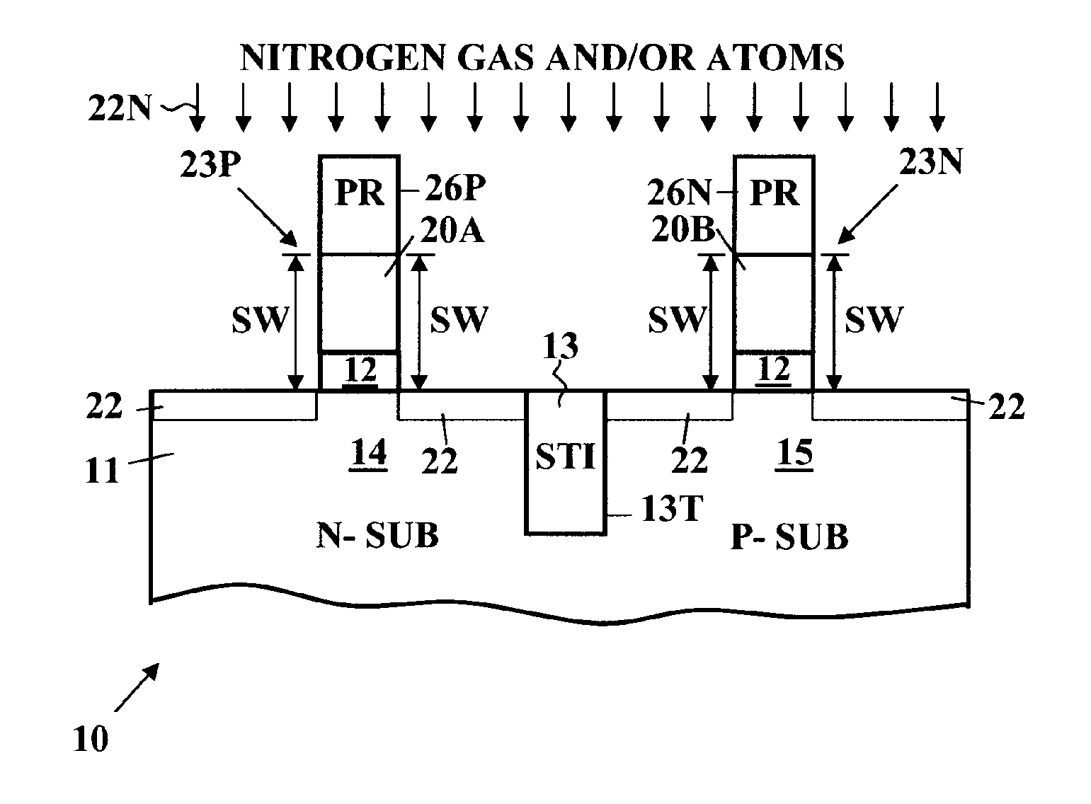
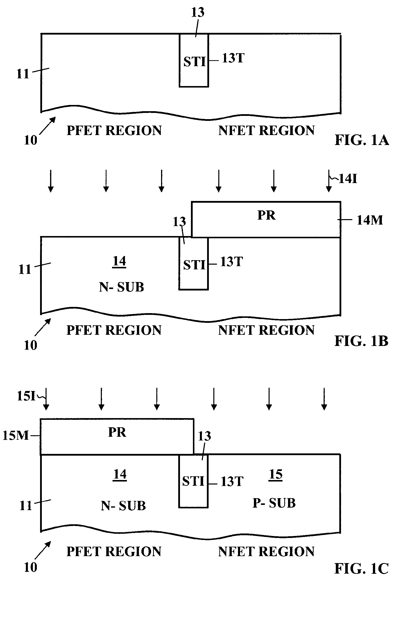
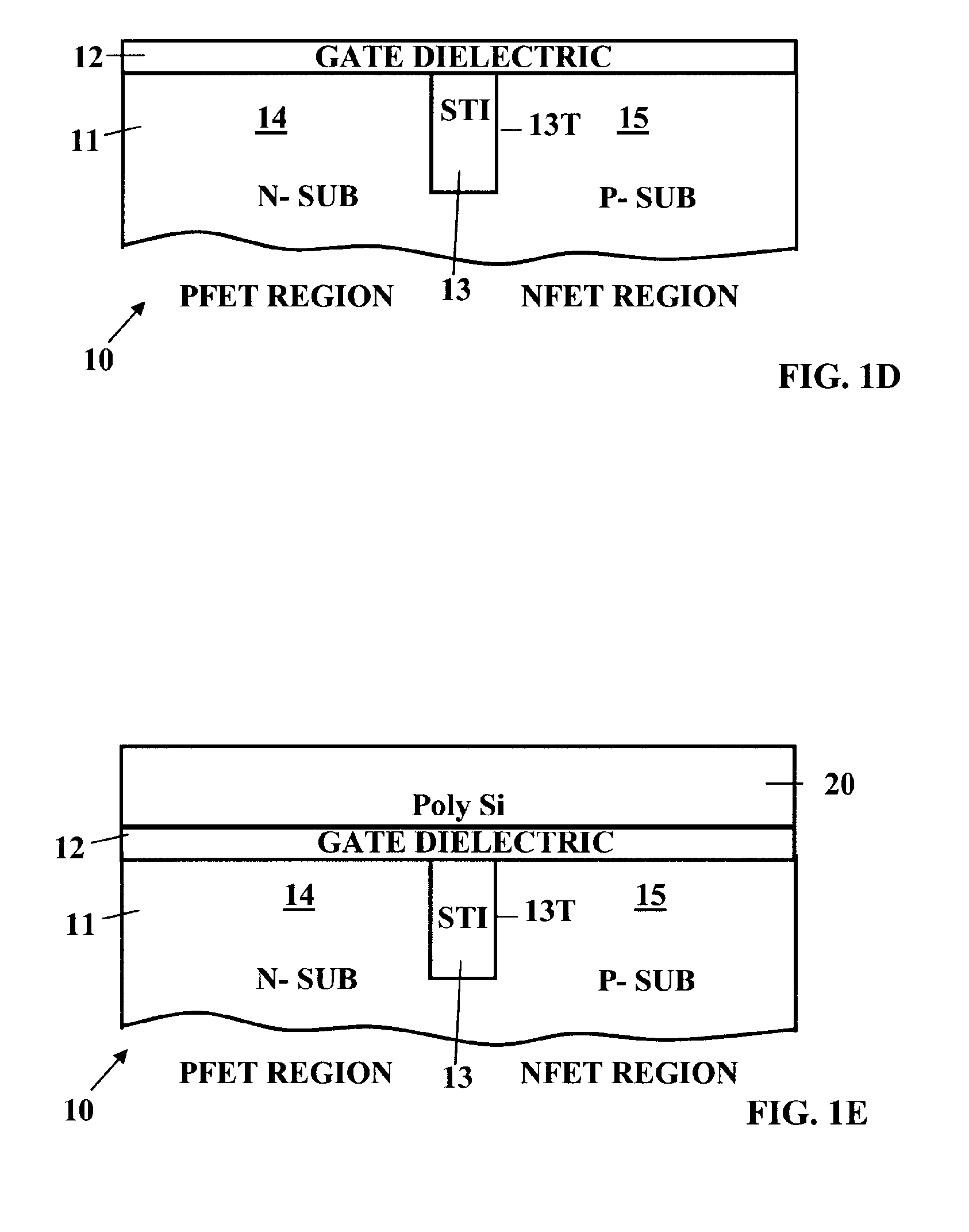
[0034]FIGS. 1A-1O show the process of forming a MOSFET device 10 in accordance with the method of this invention. FIG. 2 is a flow chart of the method of manufacture of the MOSFET device 10 in accordance with the method of this invention as illustrated by FIGS. 1A-1O.

[0035] A. Form STI Dielectric Region In An STI Trench Formed In Semiconductor Substrate

[0036]FIG. 1A is a schematic sectional view of a device 10 in an early stage of manufacture comprising a semiconductor substrate 11 with a top surface in which a shallow trench 13T has been formed. The shallow trench 13T has been filled with dielectric material forming a Shallow Trench Isolation (STI) dielectric region 13. The STI dielectric region 13 in the substrate 11 is formed in accordance with step A in FIG. 2. The STI dielectric region 13 separates the upper portion of the PFET region on the left side of the semiconductor substrate 11 from the upper portion of the NFET region on right side of semiconductor substrate 11, as wi...


PUM


Abstract

A method of formation of integrated circuit devices includes forming a gate electrode stack over a portion of a semiconductor. The stack includes a gate dielectric layer with a gate electrode thereabove. Implant diatomic nitrogen and / or nitrogen atoms into the substrate aside from the stack at a maximum energy less than or equal to 10 keV for diatomic nitrogen and at a maximum energy less than or equal to 5 keV for atomic nitrogen at a temperature less than or equal to 1000° C. for a time of less than or equal to 30 minutes. Then form silicon oxide offset spacers on sidewalls of the stack. Form source / drain extension regions in the substrate aside from the offset spacers. Form nitride sidewall spacers on outer surfaces of the offset spacers over another portion of the nitrogen implanted layer. Then form source / drain regions in the substrate aside from the sidewall spacers.

Description

BACKGROUND OF THE INVENTION [0001] This invention relates to CMOS FET devices; and more particularly to methods of manufacture of FET devices, in which offset spacers are formed prior to the steps of formation of source / drain extensions followed by formation of sidewall spacers and devices manufactured thereby. [0002] In the process of manufacture of CMOS (Complementary Metal Oxide Semiconductor) FET (Field Effect Transistor) devices (hereinafter referred to as MOSFET devices), during an intermediate point in the process gate electrode stacks of gate dielectric below and polysilicon above are formed on the top surface of a doped semiconductor substrate. Below each of the MOSFET devices, a channel will be located directly below the gate electrode in the semiconductor substrate. Subsequently, offset spacers composed of a dielectric material, e.g. silicon oxide, are formed on the vertical sidewalls of the gate electrode stacks to protect the channel below the gate electrode stack from ...

Claims


Application Information

Patent Timeline
Patent Type & Authority Applications(United States)
IPC IPC(8): H01L29/78H01L21/336
CPCH01L21/26506H01L21/28247H01L21/2658
Inventor DYER, THOMAS W.LI, JINGHONGLUO, ZHIJIONG
Owner IBM CORP
Why Eureka
Try Eureka