Semiconductor memory device, memory-mounted LSI and fabrication method for semiconductor memory device

a semiconductor memory and memory-mounted technology, applied in the field of semiconductor memory devices, can solve the problems of increasing the chip unit price and enhancing the development efficiency, and achieve the effects of preventing the increase of the chip unit price, facilitating expansion, and increasing the chip area

Inactive Publication Date: 2009-02-12
PANASONIC CORP
View PDF8 Cites 21 Cited by
  • Summary
  • Abstract
  • Description
  • Claims
  • Application Information

AI Technical Summary

Benefits of technology

[0009]An object of the present invention is providing a semiconductor memory device and a memory-mounted LSI that can be easily expanded to a variety of product types different in memory capacity with uniform characteristics being secured over the product types while preventing increase in chip unit price with increase in chip area.

Problems solved by technology

However, when it is attempted to expand a semiconductor memory device and a memory-mounted LSI to a variety of product types different in memory capacity, a photomask must be designed for each memory capacity, and this blocks enhancement in development efficiency.
In this case, however, the chip size of a product type small in memory capacity will be made to fit to the product type maximum in capacity, and this may possibly increase the chip unit price.

Method used


Image

  • Semiconductor memory device, memory-mounted LSI and fabrication method for semiconductor memory device
  • Semiconductor memory device, memory-mounted LSI and fabrication method for semiconductor memory device
  • Semiconductor memory device, memory-mounted LSI and fabrication method for semiconductor memory device

Examples


embodiment 1

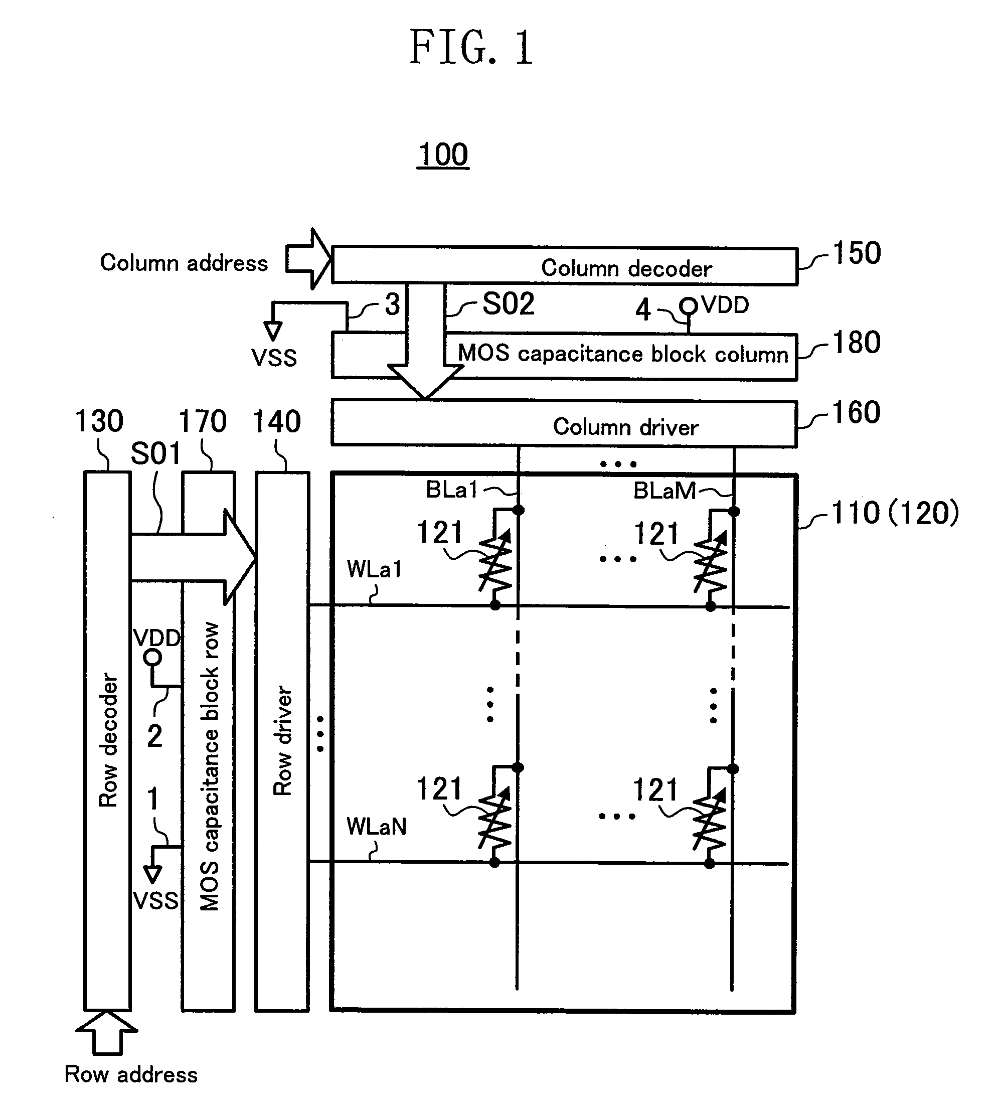
[0037]FIG. 1 is a plan view of the entire configuration of a semiconductor memory device 100 of Embodiment 1 of the present invention. One memory macro of a type greatest in memory capacity as a product (hereinafter, such a product type is called a maximum capacity product type) is designed / developed, and the memory macro is expanded to product types smaller in capacity than the maximum capacity product type (hereinafter, such product types are called small capacity product types). The semiconductor memory device 100 is one of such small capacity product types. The memory macro is provided with row drivers and column drivers of the numbers necessary for the maximum capacity product type.

[0038](Configuration of Semiconductor Memory Device 100)

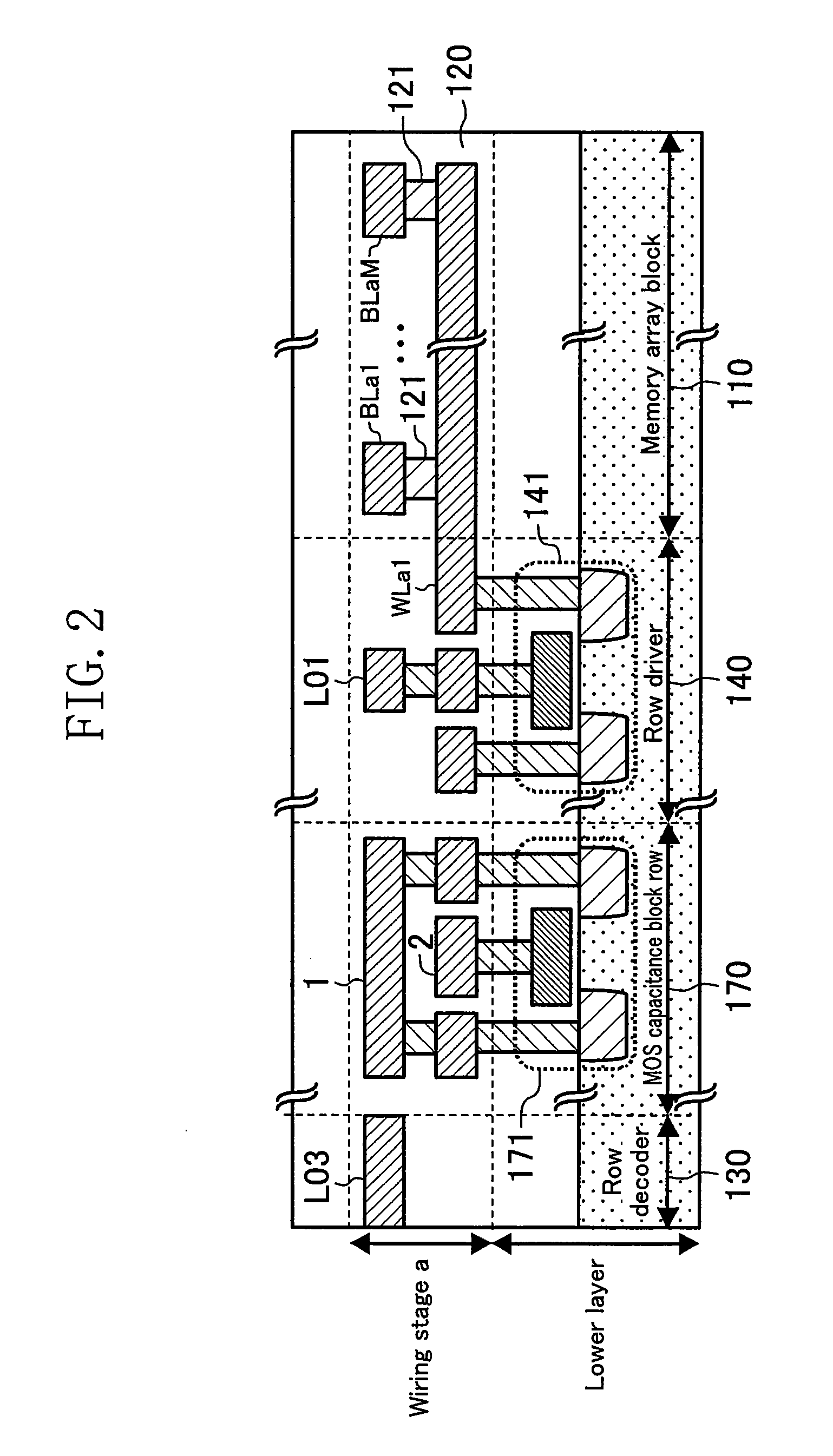
[0039]As shown in FIG. 1, the semiconductor memory device 100 includes a memory cell array block 110, a row decoder 130, a row driver 140, a column decoder 150, a column driver 160, a MOS capacitance block row 170 and a MOS capacitance block col...

embodiment 2

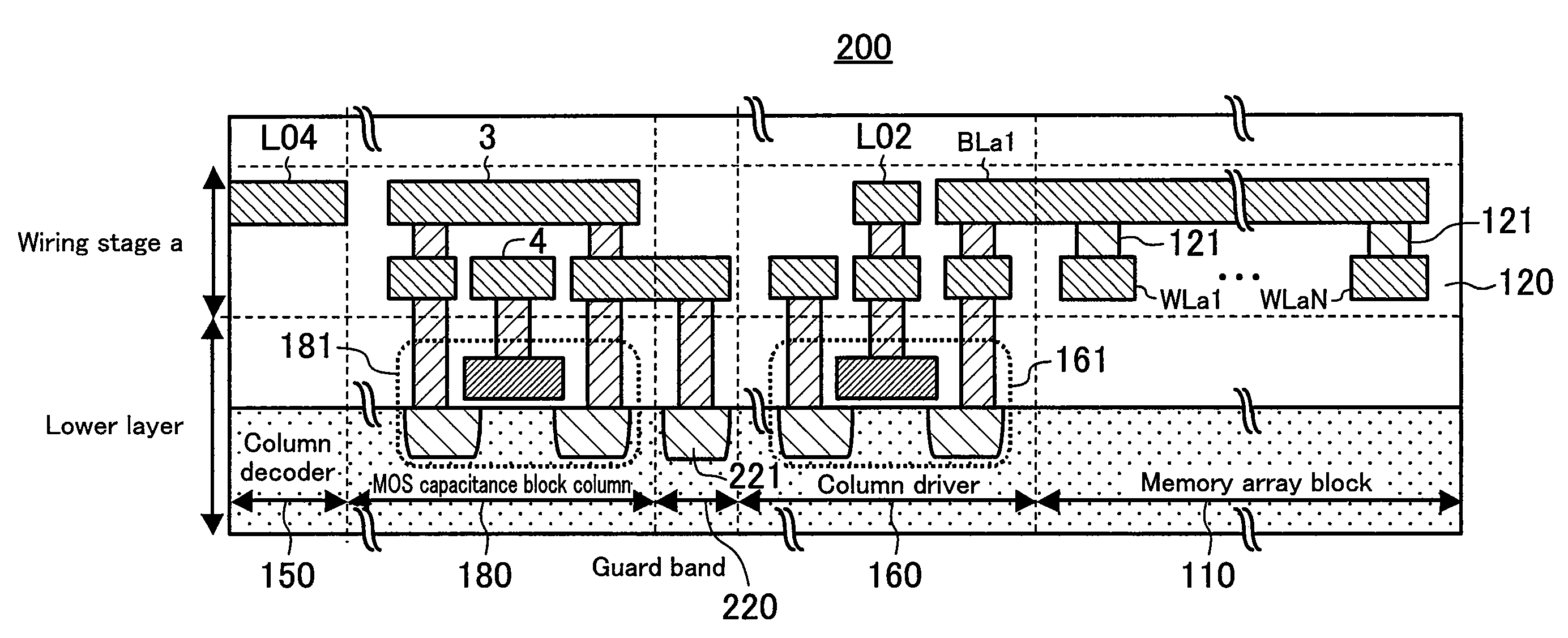
[0068]FIG. 4 is a cross-sectional view of a semiconductor memory device 200 taken along the word line WLa1. FIG. 5 is a cross-sectional view of the semiconductor memory device 200 taken along the bit line BLa1.

[0069]The semiconductor memory device 200 has a guard band 210 placed between the row driver 140 and the MOS capacitance block row 170 as shown in FIG. 4.

[0070]The guard band 210 has a channel stopper 211, which is connected with a channel for the MOS capacitor 171 (VSS1 for the source or drain). With this placement, propagation of noise due to a substrate current from the MOS transistor 141 is suppressed.

[0071]Likewise, the semiconductor memory device 200 has a guard band 220 placed between the column driver 160 and the MOS capacitance block column 180 as shown in FIG. 5.

[0072]The guard band 220 has a channel stopper 221, which is connected with a channel for the MOS capacitor 181 (VSS3 for the source or drain). With this placement, propagation of noise due to a substrate cur...

embodiment 3

Alteration to Embodiment 3

[0101]In the memory-mounted LSI 300, MOS capacitors can be used as the smoothing capacitance for power supply for an input / output circuit, for example. When the maximum voltage of the input / output circuit is higher than a voltage applied to word lines or bit lines, in particular, the thickness of the gate oxide film of the MOS transistors in the MOS transistor blocks may be made the same as the thickness of the gate oxide film of MOS transistors in the input / output circuit.

[0102]This is based on the assumption that in some cross-point memories, a voltage higher than the power supply voltage for peripheral circuits around the memory may be applied to the input / output circuit, in consideration of the voltages applied to word lines and bit lines during read and rewrite operation. For example, in dynamic RAMs (DRAMs) and some flash memories as conventional memories, some products achieve high readout speed by applying a voltage higher than the internal power su...


PUM


Abstract

The semiconductor memory device includes a memory cell array block having one or more stages of memory cell arrays stacked one on another, each memory cell array including a plurality of memory cells placed in a matrix at respective intersections of a plurality of word lines and a plurality of bit lines. A plurality of MOS transistor blocks are provided which are same in the configuration of circuit elements and include MOS transistors as one kind of the circuit elements. In part of the plurality MOS transistor blocks, the MOS transistors are used for drive of the word lines or the bit lines, while in at least part of the remaining MOS transistor blocks, the MOS transistors are used as MOS capacitors.

Description

BACKGROUND OF THE INVENTION[0001]1. Field of the Invention[0002]The present invention relates to a semiconductor memory device having cross-point memory cells, a memory-mounted LSI including such a semiconductor memory device and a circuit operating in response to data stored in the semiconductor memory device, and a fabrication method for such a semiconductor memory device.[0003]2. Description of the Prior Art[0004]In audio equipment and the like, for example, an LSI including a memory as well as a central processing unit (CPU) and a digital signal processor (DSP) (hereinafter, such an LSI is called a memory-mounted LSI) is often used. In such a memory-mounted LSI, code for an application and the like used by the CPU and the DSP are stored in the mounted memory.[0005]In such a memory-mounted LSI, it is sometimes attempted to change its function or reduce application code to hence replace the LSI with a less expensive LSI product smaller in memory capacity. In some cases, therefore,...

Claims


Application Information

Patent Timeline
Patent Type & Authority Applications(United States)
IPC IPC(8): G11C5/02G11C11/00H01L21/00
CPCB82Y10/00G11C5/025G11C8/08G11C13/00H01L27/228G11C2213/77H01L27/0629H01L27/0688G11C13/0028H10B61/22
Inventor ARAKAWA, KEN
Owner PANASONIC CORP
Why Eureka
Try Eureka